E2 - Digital Electronics
In CS1 you met the computer as an idea...a von Neumann machine with a CPU, registers, memory, and buses, stepping through a fetch-decode-execute cycle. We told you "memory is just addressable bytes" and then deliberately dodged two questions: what is actually inside a byte? and how is memory physically built?
This lesson answers both. We start from the simplest object in all of electronics, a switch that is either on or off, and we climb towards a working computer (or at least the model of one), building everything ourselves out of one kind of component: the MOSFET.
The ladder that we are about to climb looks like this:
MOSFET switch -> logic gates -> arithmetic & memory -> CPU
Nothing in a computer is magic. It is one tiny switch, repeated a few billion times (up to hundreds of billions of times these days) and wired together. By the end you should be able to read a truth table, build the basic gates out of transistors, explain how a circuit can add and how a circuit can remember, and see how it all assembles into the kinf of machine you learned about in CS1. The microcontroller you will solder onto your AirBox station is exactly such a machine - so this is not abstract trivia, it is the thing in your hands.
From analog to digital
The world is analog: temperature, sound, the voltage on a wire - all of them vary smoothly and can take any value. Analog is natural, but it has a fatal weakness for building reliable machines: noise. Every wire picks up interference, every copy of a signal is slightly degraded, and those errors accumulate. Push an analog value through a hundred stages and you no longer know what it was.
Digital electronics makes one radical simplification. Instead of allowing any value, we allow only two: a low level (call it 0) and a high level (call it 1), with a deliberately empty forbidden zone between them. On a 3.3 V system, anything near 0 V means 0 and anything near 3.3 V means 1; the middle is "don't care." Now noise barely matters: as long as the interference is smaller than the gap, every stage can regenerate the signal - snap it cleanly back to a crisp 0 or 1. That single property, noise immunity, is why digital beat analog, and why you can build a trustworthy computer out of billions of imperfect parts.
So a digital signal is just two voltage levels. What we need next is a component that can be switched cleanly between those two levels by another signal. That component is the MOSFET.
The Diode: one-way conductor
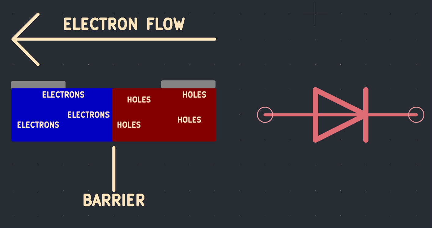
The diode is a component that only allows current to flow in one direction. It contains two doped Silicon areas, with opposite charges.
- P-Type areas - material that has less electrons than Silicon (positive,
HOLES), made by adding Boron or Aluminium. - N-Type areas - material that has more electrons than Silicon (negative,
ELECTRONS), made by adding Phosphorus or Arsenic.
 |
|---|
| Diode construction. Electron pressure from the P-Type area towards the N-Type area will cause the barrier to lose differential, therefore allowing current to pass through. |
Polarizing the diode in the reverse direction causes even more electrons to accumulate in the N-Type section, further strengthening the barrier, therefore no current can flow.
If the pressure (voltage) applied is too high, the whole semiconductor can break down, allowing a huge current to flow through, accompanied by large amounts of heat and smoke. The diode is permanently damaged.
The MOSFET: a voltage-controlled switch
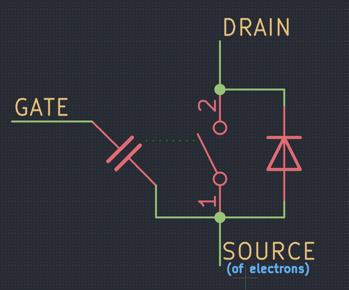
The only component we use in this whole lesson is the MOSFET. It has three terminals that matter to us: the gate, the source, and the drain. The key facts:
- The gate is electrically insulated from the rest of the device. Almost no current flows into the gate - it is a voltage-sensing terminal. You don't drive it with current; you just present a voltage to it.
- That gate voltage decides whether current is allowed to flow between source and drain. High enough gate voltage → a conducting channel forms → current can flow (switch closed, ON). Remove the voltage → the channel vanishes → no current (switch open, OFF).
 |
|---|
| MOSFET equivalent schematic |
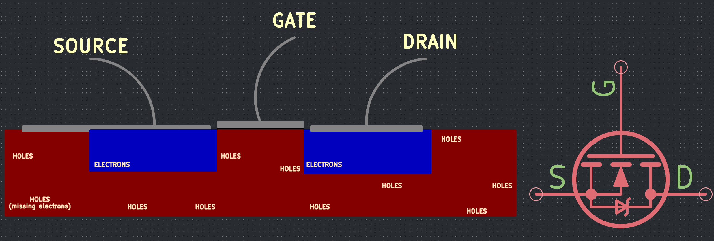
MOSFETS are built using semiconductor material, notably three kinds of areas:
- P-Type areas -
HOLES - N-Type areas -
ELECTRONS - Oxide - electrical isolator created by oxidizing Silicon into SiO2.
You fabricate a MOSFET by creating two wells of inversely doped material in a semiconductor substrate, depositing a thin SiO2 layer under the gate, and bonding all three components with conductors.
Depending on what polarity the substrate has, we can build two types of MOSFETS:
- NMOS has a P-Type substrate and N-Type wells. It conducts by creating an electron-rich channel.
- PMOS has a N-Type substrate and P-Type wells. It conducts by creating an electron-depleted channel, identical to its two wells. Because of the lack of electrons, it has to only rely on the natural conductivity of the P-Type material, therefore conducts electricity worse than NMOS variants. Due to the inverse doping, the voltage applied must be reversed (negative).
Due to PMOS's reduced conductivity and negative Gate-Source voltage requirement, designers prefer NMOS and use PMOS only when necessary.
 |
|---|
| NMOS transistor internal construction in unpowered state |
 |
|---|
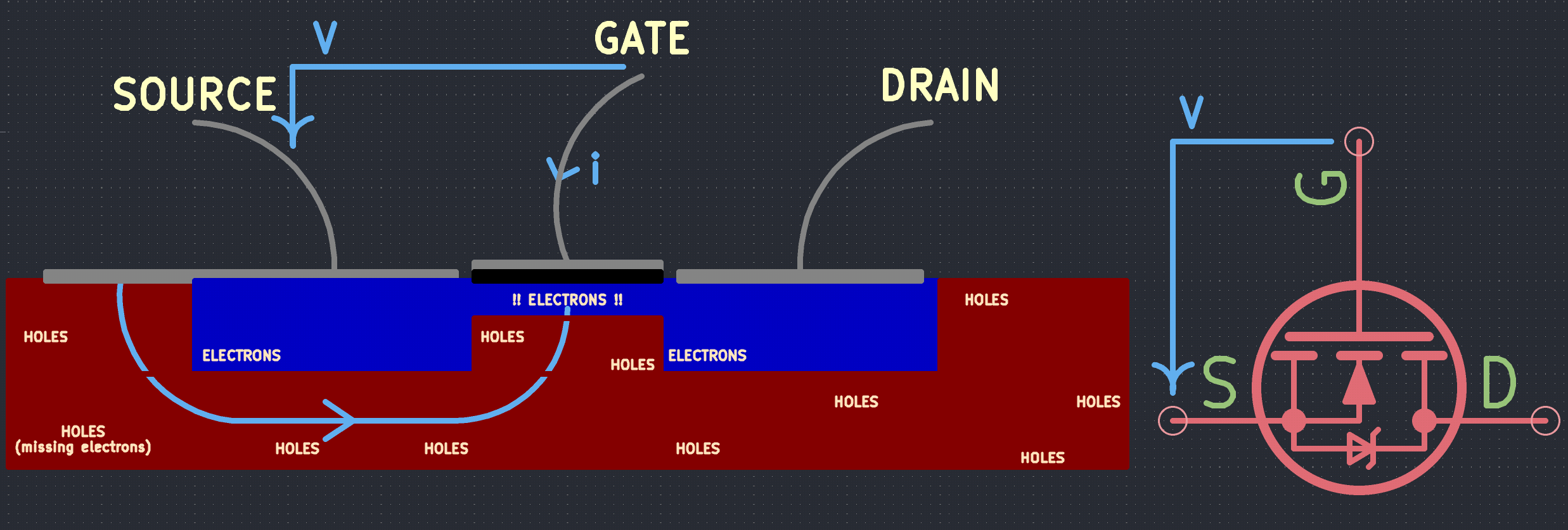
| NMOS transistor with a voltage applied across Gate-Source The current moves electrons through the P-Type substrate towards the dielectric, where they accumulate and create a temporary N-Type area. This continuous area allows current to flow from Drain to Source. |
The Drain, together with the substrate-connected Source, form a PN junction that behaves like a diode across the MOSFET. Therefore, MOSFETS conduct in one direction when unpowered, and in both directions when powered.
The voltage needed to open the MOSFET depends on the physical dimensions and properties of the N-Type and P-Type areas in the die. Datasheets list this value as VGS(th).
That is the entire idea: a voltage on the gate opens or closes a switch between the other two terminals, and the gate itself draws essentially no current except the initial inrush current caused by the gate capacitance. No moving parts, switches billions of times a second, never wears out. (This is the "field effect": the gate's electric field pulls the channel into existence)
Logic inputs and outputs
A logic level is a voltage on a wire that the circuit reads as 0 or 1. Gates pass logic levels to each other through two operations: an output that writes a level onto a wire, and an input that reads it.
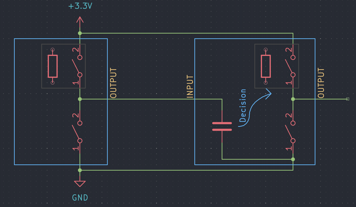 |
|---|
| An output stage (left) driving an input stage (right). The "Decision" is the receiving MOSFET's threshold comparison. |
Writing a level (left half). The output node sits between two switches and two rails. The bottom switch is an NMOS: close it and it pulls the output to GND through the MOSFET's milliohm-scale on-resistance, writing a hard 0. The top path connects the output to +3.3 V through a pull-up resistor, so when the bottom switch is open, the resistor pulls the output high, writing a 1. In a real CMOS chip, a PMOS transistor replaces the resistor; we use a resistor because it is simpler and behaves the same way for logic.
Reading a level (right half). The output wire connects to the next MOSFET's gate. Gate oxide insulates the gate from the channel, forming a tiny capacitor: the arriving voltage charges it. The second device compares the stored voltage against its threshold VGS(th) and executes its internal logic. Only a brief inrush of current flows while the capacitor charges to the new level; after that, the gate draws nothing.
Follow what happens at the output when the bottom NMOS opens and closes:
-
Switch closes (input goes high, output falls). The NMOS turns on and connects the output to GND through milliohms of resistance. The output voltage drops fast, nearly vertical on the waveform. Fall time depends on the MOSFET's on-resistance, and good MOSFETs keep that in the milliohm range, so the fall is short and fixed.
-
Switch opens (input goes low, output rises). The NMOS turns off. Only the pull-up resistor can charge the output back toward +3.3 V, and it must do so through the load capacitance (the next gate's gate capacitor, plus parasitic wire capacitance). The voltage rises along an RC curve: an exponential approach to 3.3 V, with a time constant set by R and the total C. The rise time depends on the resistor value.
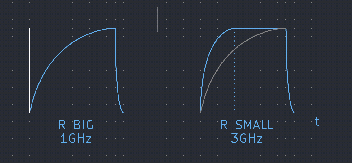 |
|---|
| Output waveforms for two resistor values. Left: large R, slow rise, 1 GHz maximum. Right: small R, faster rise, 3 GHz maximum. Fall time is the same in both. |
Because the rise time depends on R and the fall time does not, you face a direct tradeoff between power and speed.
A large resistor (left waveform) limits current, so the circuit wastes less power when the NMOS is on. But the RC time constant grows with R, slowing the rising edge. At some point the output cannot finish rising before the next clock edge arrives: you hit the maximum operating frequency. In the figure, the large resistor caps the circuit at about 1 GHz (example).
A small resistor (right waveform) charges the capacitor faster, producing a steeper rise and a higher usable frequency (3 GHz in the figure). More current flows through the resistor whenever the NMOS pulls the output low. All of that current becomes heat. Halve R and you double the wasted power.
The fall time stays the same in both cases. The MOSFET's on-resistance sits in the milliohm range regardless of the pull-up resistor, so the falling edge is always fast. Only the rising edge moves.
NMOS vs PMOS (application note)
To actually see a level come out, you wire the MOSFET in series with a load. Here the load is just a resistor between the switch and the opposite power rail:
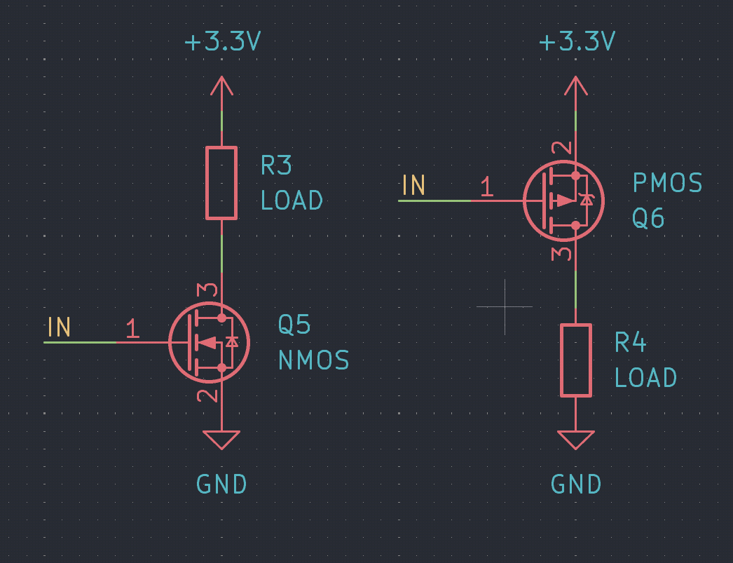 |
|---|
| An NMOS (left) and a PMOS (right), each in series with a load resistor between +3.3 V and GND. The MOSFET is the switch; the resistor is what turns "switch open/closed" into a readable voltage. |
When the switch is open, no current flows through the load, so the output sits at the rail the resistor connects to. When the switch closes, current flows and pulls the output to the other rail.
- NMOS turns ON when its gate is HIGH (1). It is best at connecting its output down to GND - a good low-side (pull-down) switch. In the figure above, the NMOS sits below its load.
- PMOS turns ON when its gate is LOW (0) - the opposite. It is best at connecting its output up to +3.3 V - a good high-side (pull-up) switch. In the figure, the PMOS sits above its load.
In this lesson we build our gates from NMOS plus a pull-up resistor, because it is the simplest thing that works and easiest to reason about.
Modern fabrication techniques have perfected the art of creating precision MOSFETS, both NMOS and PMOS. A lithography machine can produce millions of transistors on the same wafer, but resistors are much harder to manufacture at microscopic scale.
Therefore, in modern chips, CMOS circuitry (Complementary - Both NMOS and CMOS) are preferred instead of NMOS-Resistor logic.
Building logic gates from MOSFETs
Now we compute. A logic gate takes one or two bits in and produces one bit out, and its complete behaviour is captured by a truth table - a list of the output for every possible input. This algebra of 1s and 0s is Boolean algebra (George Boole, 1850s, long before any electronics existed).
The recipe for every gate below is the same: a network of NMOS switches between the output and GND, plus a pull-up resistor to +3.3 V. If the NMOS network finds a path to GND, the output is pulled low (0); if not, the resistor holds it high (1). Arrange the NMOS cleverly and you get any logic you want.
NOT (the inverter)
The simplest gate. One NMOS, one pull-up resistor:
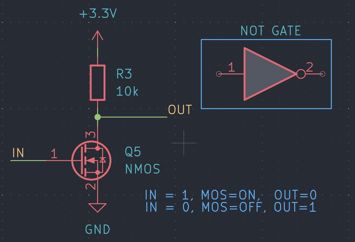 |
|---|
| NOT: the output sits between the pull-up resistor (to +3.3 V) and a single NMOS (to GND). |
Follow the current:
- IN = 0 → the NMOS is OFF. No path to GND exists, so no current flows through the resistor, there is no voltage drop across it, and the output is pulled all the way up to 3.3 V → OUT = 1.
- IN = 1 → the NMOS is ON. Now there is a path to GND, so a small current flows from +3.3 V, through the resistor, through the NMOS, to ground. That current drops almost the entire 3.3 V across the resistor, leaving the output near 0 V → OUT = 0.
The resistor defines the "high" level and limits the current that flows when the switch is closed.
| A | NOT A |
|---|---|
| 0 | 1 |
| 1 | 0 |
NAND (two NMOS in series)
Stack two NMOS one above the other (in series) between the output and GND:
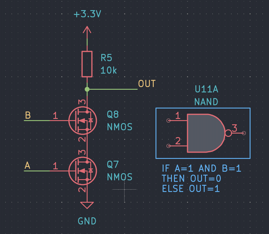 |
|---|
| NAND: two NMOS in series. Current only reaches GND if both are ON. |
A series path conducts only if every switch in it is closed. So the output is pulled low only when A = 1 AND B = 1; in every other case at least one NMOS is open, no path exists, and the resistor holds the output high. That is NAND ("not AND"):
| A | B | NAND |
|---|---|---|
| 0 | 0 | 1 |
| 0 | 1 | 1 |
| 1 | 0 | 1 |
| 1 | 1 | 0 |
AND (a NAND followed by a NOT)
There's no simple all-NMOS gate that pulls low when both inputs are low; the natural NMOS gates come out inverted (NAND, NOR). So to get a plain AND, we take the NAND we just built and invert it with the NOT from before:
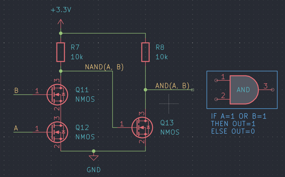 |
|---|
| AND = NAND then NOT. The first stage produces NAND(A, B); a second inverter stage flips it into AND(A, B). |
AND(A,B) = NOT(NAND(A,B)). Two stages, and now the output is 1 only when both inputs are 1:
| A | B | A AND B |
|---|---|---|
| 0 | 0 | 0 |
| 0 | 1 | 0 |
| 1 | 0 | 0 |
| 1 | 1 | 1 |
NOR (two NMOS in parallel)
Now put the two NMOS side by side (in parallel) instead of stacked:
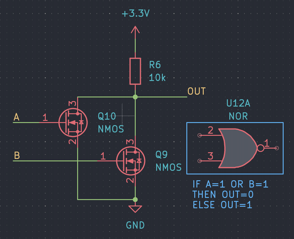 |
|---|
| NOR: two NMOS in parallel. Either one ON is enough to reach GND. |
A parallel path conducts if any switch is closed. So the output is pulled low whenever A = 1 OR B = 1, and only stays high when both are 0. That is NOR ("not OR"):
| A | B | NOR |
|---|---|---|
| 0 | 0 | 1 |
| 0 | 1 | 0 |
| 1 | 0 | 0 |
| 1 | 1 | 0 |
Notice the symmetry you now have: NMOS in series → NAND, NMOS in parallel → NOR. That's the core grammar of building logic out of switches.
XOR (the "are they different?" gate)
XOR ("exclusive OR") outputs 1 exactly when the two inputs differ. It's the most useful gate for what comes next, and it can't be done in one tidy stage - you build it from the gates you already have. The classic recipe uses four NANDs:
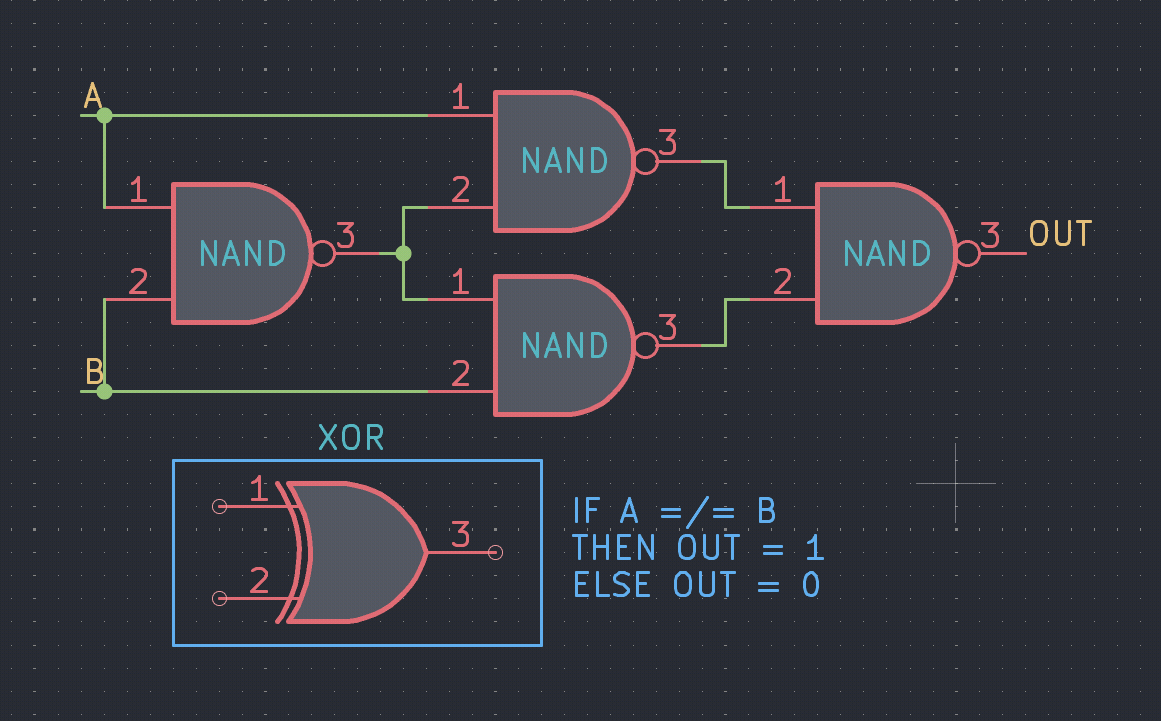 |
|---|
| XOR at the gate level: four NANDs wired so the output is 1 only when A and B differ. |
And because every one of those NANDs is itself just NMOS and a resistor, you can "unfold" the whole thing into raw transistors - this is the same XOR, expanded all the way down:
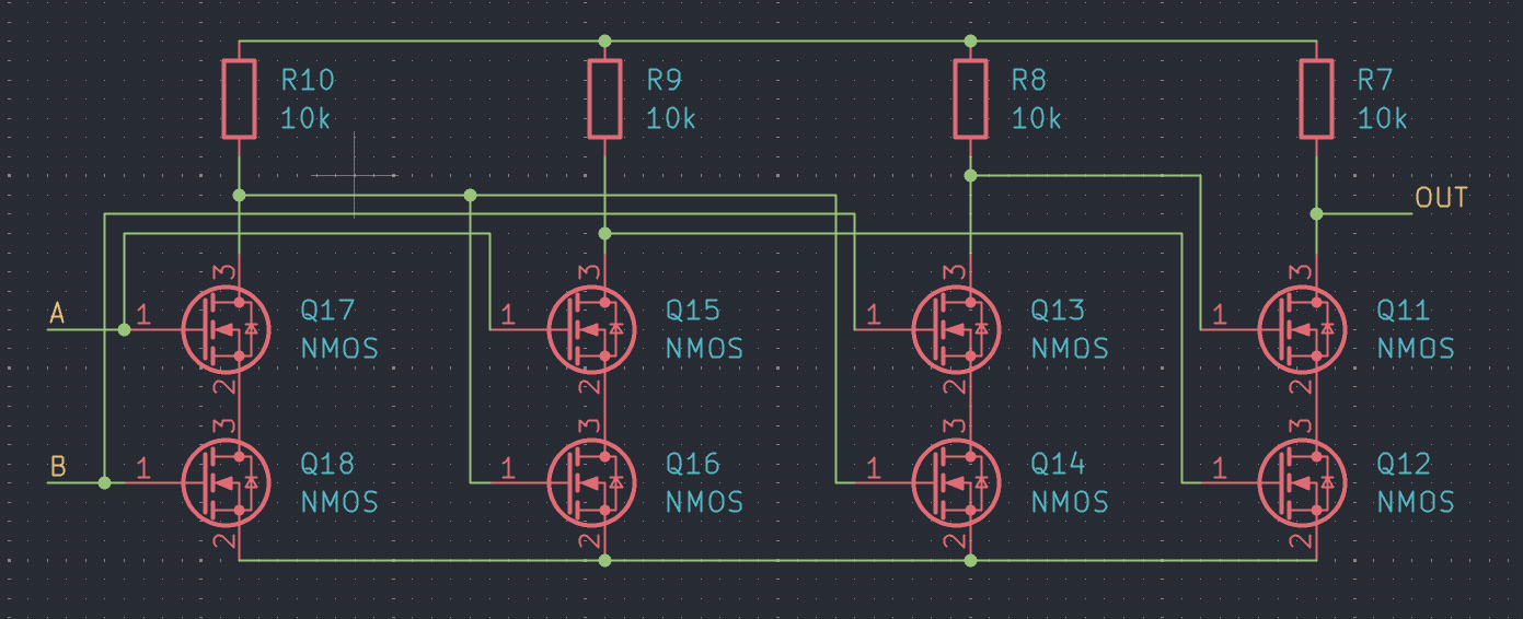 |
|---|
| The same XOR, drawn as the MOSFETs and pull-up resistors it's really made of. Gates are a convenient shorthand; underneath, it's all switches. |
| A | B | XOR |
|---|---|---|
| 0 | 0 | 0 |
| 0 | 1 | 1 |
| 1 | 0 | 1 |
| 1 | 1 | 0 |
Keep your eye on XOR = "are these two bits different?" - it is the heart of binary addition, which we reach when we build the adder.
One gate to rule them all
You just saw AND built from NAND + NOT, and XOR built from NANDs. This is no accident: every logic function can be built from NAND gates alone (NOR works too). Tie a NAND's inputs together and you get NOT; NAND-then-NOT gives AND; and so on. Since NOT, AND, and OR are enough to build anything, and all three come from NAND, NAND alone is enough to build an entire computer. That's exactly why your homework game is called NandGame.
A useful tool for rearranging gates is De Morgan's laws, which trade ANDs for ORs through NOT:
NOT (A AND B)  =  (NOT A) OR  (NOT B)
NOT (A OR  B)  =  (NOT A) AND (NOT B)
They're the formal reason you can always re-express a circuit in pure NANDs.
Counting in a computer: binary, hexadecimal, two's complement
Before we make the gates do arithmetic, we need to know what the bits mean. A computer has two voltage levels, so it counts in base 2 - binary.
Binary
In everyday base 10, the digits of 253 mean 2×100 + 5×10 + 3×1 - powers of ten. Binary is the same idea with powers of two. The place values are … 32 16 8 4 2 1. One binary digit is a bit; four bits are a nibble; eight bits are a byte.
Binary → decimal - add up the place values where there's a 1:
1 0 1 1 = 1×8 + 0×4 + 1×2 + 1×1 = 8 + 2 + 1 = 11
Decimal → binary - repeatedly divide by 2 and read the remainders bottom-to-top:
13 ÷ 2 = 6  r 1
 6 ÷ 2 = 3  r 0
 3 ÷ 2 = 1  r 1
 1 ÷ 2 = 0  r 1      →  read up  →  1101   (check: 8+4+1 = 13 ✓)
An 8-bit byte therefore holds values from 0000 0000 = 0 to 1111 1111 = 255: 256 distinct values.
Hexadecimal
Long strings of bits are miserable to read, so we use hexadecimal (base 16) as shorthand. Its sixteen digits are 0-9 then A B C D E F for ten to fifteen. The magic: one hex digit is exactly four bits (one nibble), so binary ↔ hex is just grouping by four - no arithmetic:
1011 0110₂   →   B    6   →   0xB6      (and 0xB6 = 11×16 + 6 = 182)
(1011 = B)      (0110 = 6)
This is why memory addresses and byte values are written in hex everywhere - and why, in CS2, the addresses your pointers hold will look like 0x7ffd....
Characters and negatives
Text is numbers too: a code such as ASCII assigns 'A' = 65 = 0x41, 'a' = 97, '0' = 48. So the char type from CS1 is literally a small integer.
Negative numbers use a scheme called two's complement, chosen so that the same adder we build next works for both positive and negative values - no separate subtractor. An 8-bit two's-complement byte spans −128 to +127.
For how two's complement is formed and why the arithmetic just works, see Two's complement on Wikipedia. For how decimals (floats) are stored, see IEEE 754.
Building an adder
We have gates; the bits mean numbers; now let's make the gates add. A circuit whose output depends only on its current inputs (no memory) is combinational - the gates section and this one are both combinational.
The half-adder, and what "carry" is
Add two single bits and write the answer in binary. Three of the four cases are obvious; the surprise is 1 + 1. In decimal, 7 + 5 = 12: you write the 2 and carry the 1 into the next column. Binary does the same - 1 + 1 = 10: you write a 0 and carry a 1 into the next (twos) column. The carry is simply the overflow that doesn't fit in this column and has to move to the next one.
So adding two bits needs two outputs: the Sum bit for this column and the Carry bit for the next.
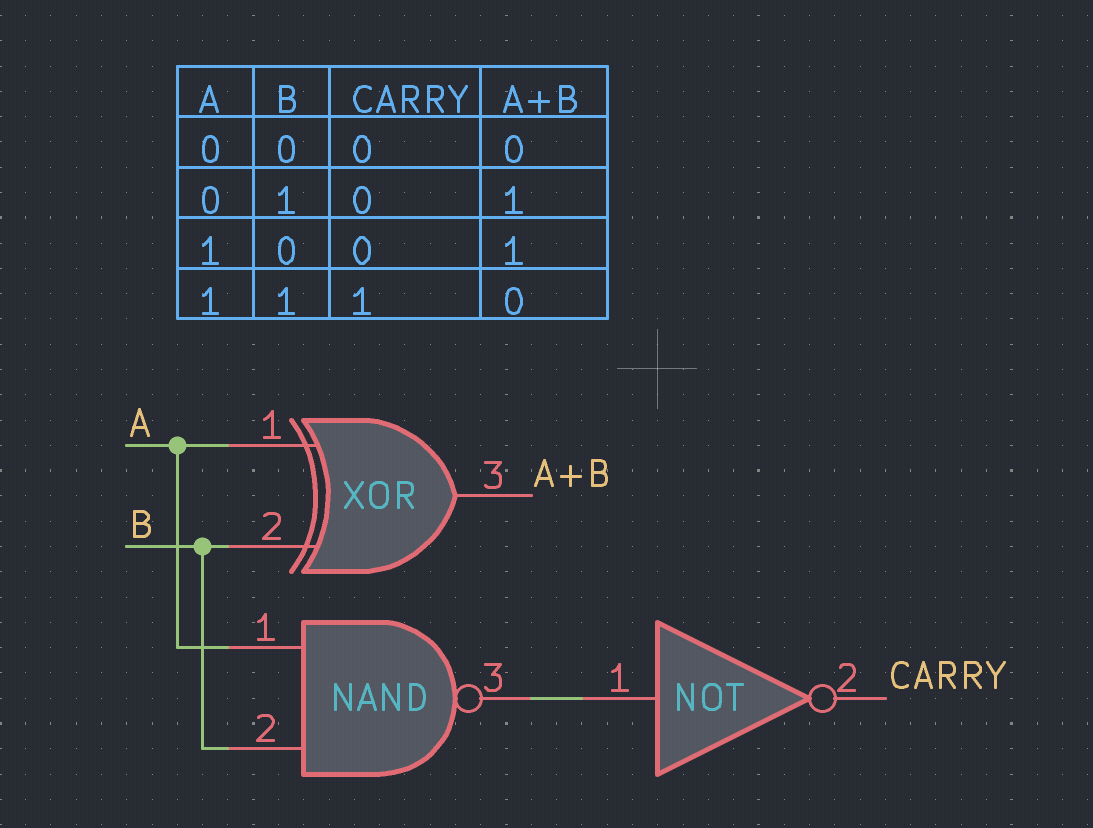 |
|---|
| Half-adder. Sum = A XOR B (1 when the bits differ); Carry = A AND B (1 only when both are 1). |
Look at the truth table in the figure: Sum is 1 exactly when the inputs differ - that's XOR. Carry is 1 only when both are 1 - that's AND. (The figure builds that AND, as before, from a NAND followed by a NOT.)
Sum   = A XOR B
Carry = A AND B
This is a half-adder: it produces a carry out, but it has nowhere to accept a carry coming in from a lower column. For real multi-bit addition we need that.
The full-adder (two half-adders + an OR)
A full-adder adds three bits: A, B, and a carry-in from the column below - producing a Sum and a carry-out. The neat part: a full-adder is just two half-adders chained, with an OR to combine the two possible carries.
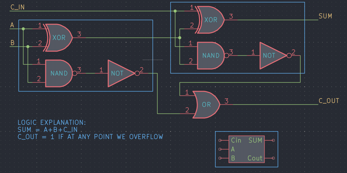 |
|---|
| Full-adder: the first half-adder adds A + B; the second adds the carry-in; an OR gate merges the carries. Carry-in + A + B → Sum + carry-out. |
The first half-adder adds A and B. The second adds the carry-in to that result, giving the final Sum. A carry-out happens if either addition overflowed, so the two carries are OR-ed together. In short: Cin + A + B → Sum + Cout.
The multi-bit (ripple-carry) adder
To add real numbers, line up one full-adder per bit and chain each carry-out into the next column's carry-in. The carry "ripples" from the lowest bit up to the highest:
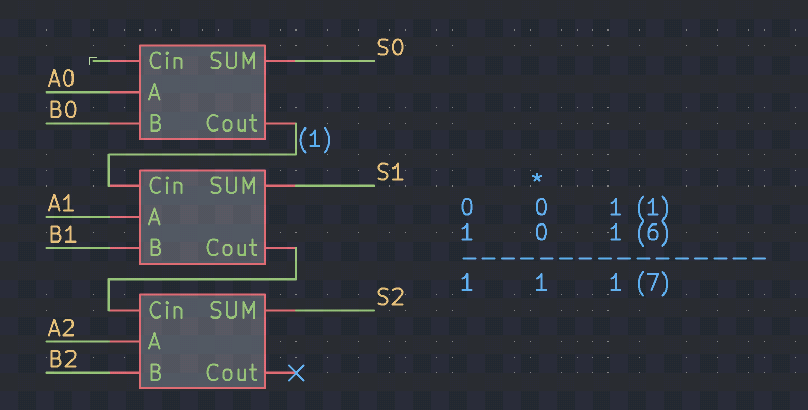 |
|---|
| A 3-bit adder: three full-adders, each carry feeding the next. Worked example: 1 + 6 = 7 (001 + 110 = 111). |
Widen this to 8, 32, or 64 bits and you have the arithmetic core of a CPU's ALU. And it subtracts for free: because negatives are stored in two's complement, A − B is just A + (−B) fed through the very same adder. One circuit, both operations.
Two's complement, concretely. To make a number negative you invert every bit and add 1 - that turns
Binto−B. So the same adder also subtracts: feed itA, the invertedB, and a carry-in of 1, i.e.SUB = A + INV(B) + 1.
Example, 5 − 3 in 4 bits: −3 =INV(0011) + 1=1100 + 1=1101. Then0101 (5) + 1101 (−3)=1 0010→ discard the carry-out →0010= 2. ✓
The lowest full-adder's carry-in supplies that "+1" for free; the final carry-out is simply dropped.
Memory: making a circuit remember
Everything so far forgets instantly - change the inputs and the outputs change with them. A computer must remember: hold a value after the inputs that set it are gone. The trick is feedback - wire an output back around into an input so the circuit "holds its own hand."
The RS latch
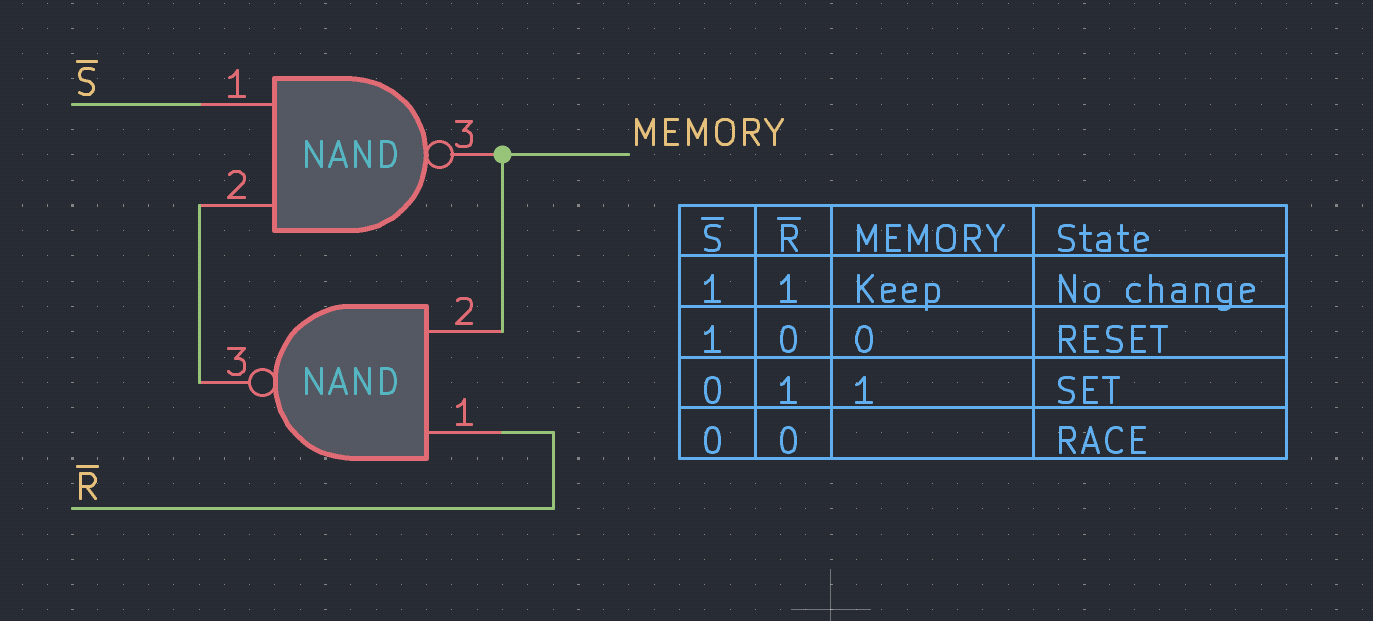
Cross-couple two NAND gates - each one's output feeds the other's input - and you get the simplest one-bit memory, the RS latch:
 |
|---|
| RS latch (NAND version). Inputs are active-low (S̄, R̄). The output holds its last value when both inputs are 1. |
Read the state table in the figure:
- S̄ = 0, R̄ = 1 → SET: output forced to 1.
- S̄ = 1, R̄ = 0 → RESET: output forced to 0.
- S̄ = 1, R̄ = 1 → KEEP: the latch holds its last value. This is memory - the bit persists with nothing actively driving it.
- S̄ = 0, R̄ = 0 → RACE: forbidden. Both NANDs are driven at once and the result is inconsistent.
This works, but it's awkward to use, and that's the important lesson. The inputs are active-low (you SET by pulling a line to 0, which is backwards from how you'd think), and there's that forbidden RACE state waiting to bite you if both inputs ever go low together. Driving an RS latch safely and conveniently takes care. We'd much rather have a memory cell with one clean "data" input.
The D latch
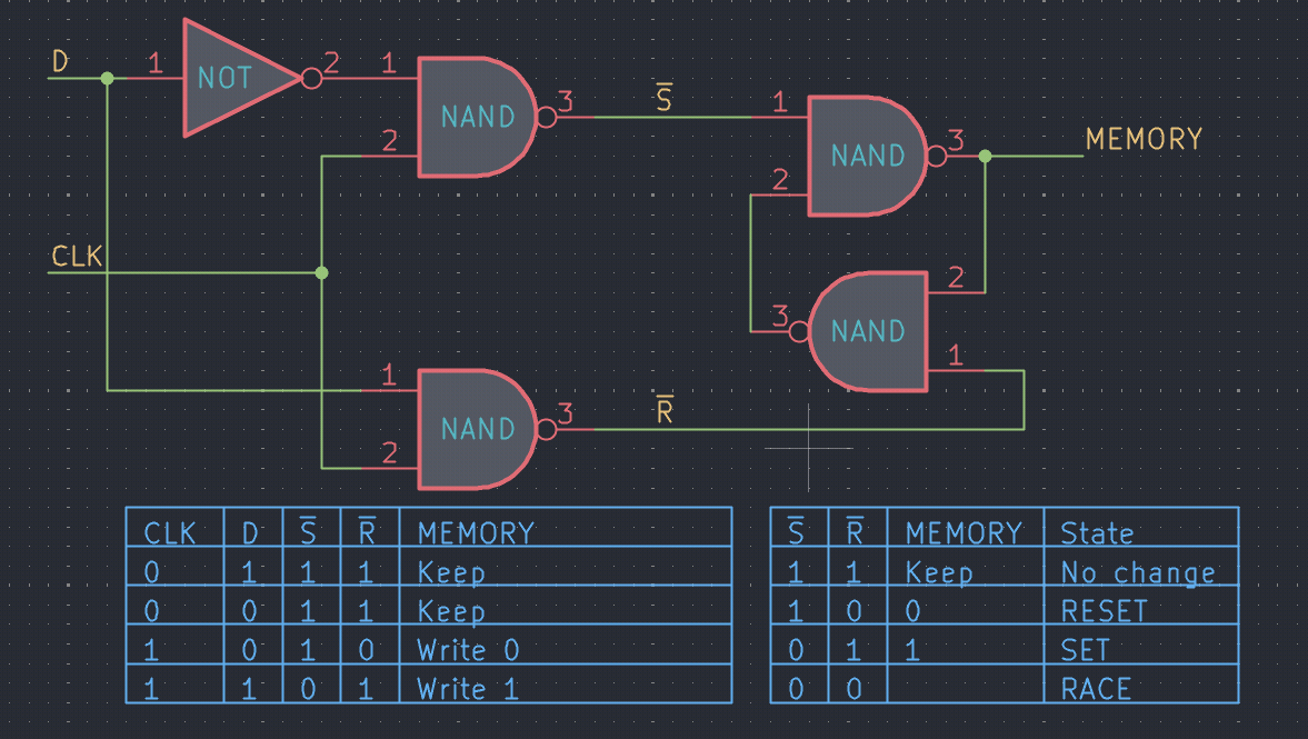
The fix: keep the reliable RS latch as the storage core, but bolt a small front-end onto it that turns a single data input D into a safe pair of S̄/R̄ signals - and only lets a write happen when a clock says so.
 |
|---|
| D latch. When CLK is high, D is translated into the SET/RESET pair (write D); when CLK is low, the RS core is told to keep. The dangerous 00 state can never occur. |
Trace the two cases in the figure's truth table:
- CLK = 1 (high): the front-end transforms D into the RS scheme.
D = 1produces SET (write a 1);D = 0produces RESET (write a 0). The latch simply stores whatever D is. - CLK = 0 (low): the front-end forces S̄ = R̄ = 1, the KEEP state - so D is ignored and the stored bit is held.
Two wins fall out of this. First, you now write memory with one obvious data line plus a clock, instead of fiddly active-low set/reset. Second - and this is the elegant part - the front-end can never present S̄ = R̄ = 0, so the forbidden RACE state is designed out of existence. The D latch is a proper, safe, one-bit memory cell.
We build with latches. A latch like this is about as simple as storage gets - just a handful of gates - which makes it cheap to lay down in silicon. Typically latches are easier to implement in hardware than fancier storage elements, so wherever a design can use a plain latch it generally should: it is the more area- and power-efficient choice. The D latch is our one-bit memory cell for the rest of this lesson.
From latch to register to memory
- Put N D latches side by side, sharing one clock, and you store an N-bit word: a register (exactly the CPU registers from CS1).
- Stack many words and add a decoder that turns an address into "select this one word," and you have addressable memory. That's the literal answer to CS1's deferred question:
An address is just the number you feed into a decoder that selects one row of latches.
Real RAM (DRAM) swaps each latch for a far denser cell - one transistor and one tiny capacitor per bit - so billions fit on a chip, but the principle is identical: an address goes through decoding logic to pick one location.
Selecting data: the multiplexer, and a memory bank
Our memory cell holds one bit and a register holds a word - but a useful memory has many locations, and we need to pick one to read or write. The tool for picking is the multiplexer (mux): a circuit that passes one of several inputs through to its output, chosen by some select bits. Let's build it, scale it, then use it together with our D latches to make a small read/write memory.
The multiplexer, from gates
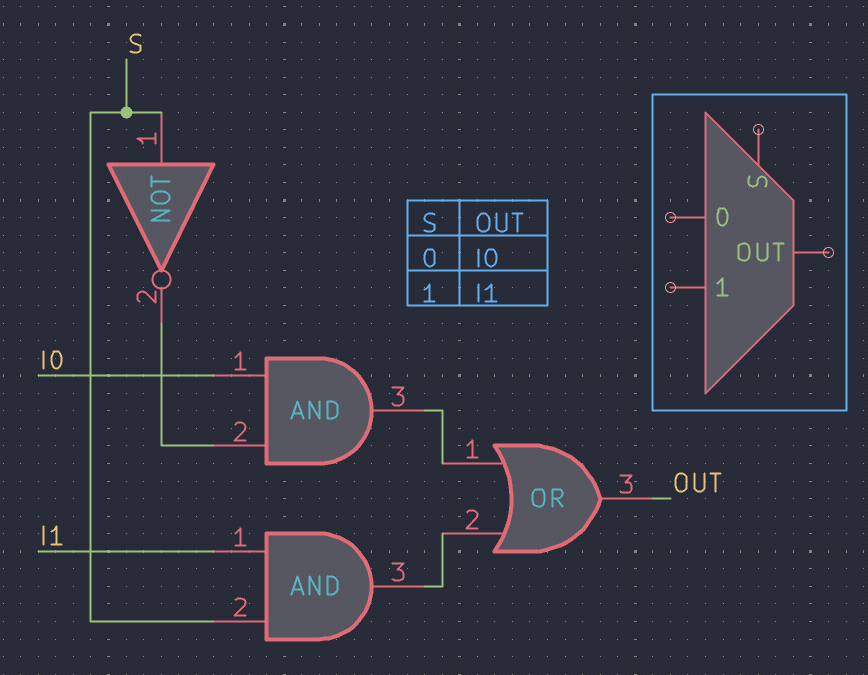
The simplest mux is 2-to-1: two data inputs I0 and I1, one select line S, one output. S = 0 passes I0; S = 1 passes I1:
 |
|---|
A 2:1 mux: OUT = (I0 AND NOT S) OR (I1 AND S). The select line opens exactly one input's AND gate; the OR collects whichever is open. |
Read it as two gated doors: when S = 0, NOT S = 1 opens I0's gate while I1's is forced to 0; when S = 1 the roles swap.
| S | OUT |
|---|---|
| 0 | I0 |
| 1 | I1 |
Bigger muxes from smaller ones
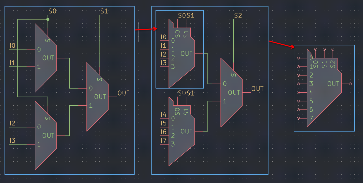
To choose among more inputs, add select bits and stack muxes. A 4-to-1 mux is just three 2:1 muxes: one picks I0/I1, another picks I2/I3 (both steered by S0), and a final mux picks between those two results (steered by S1):
 |
|---|
Three 2:1 muxes make a 4:1 mux (selects S0, S1). Repeat the trick - two 4:1 muxes feeding a 2:1 mux make an 8:1 mux (S0, S1, S2). |
The pattern is general: each extra select bit doubles the inputs you can choose from - n select bits select among 2ⁿ inputs.
A read/write memory bank
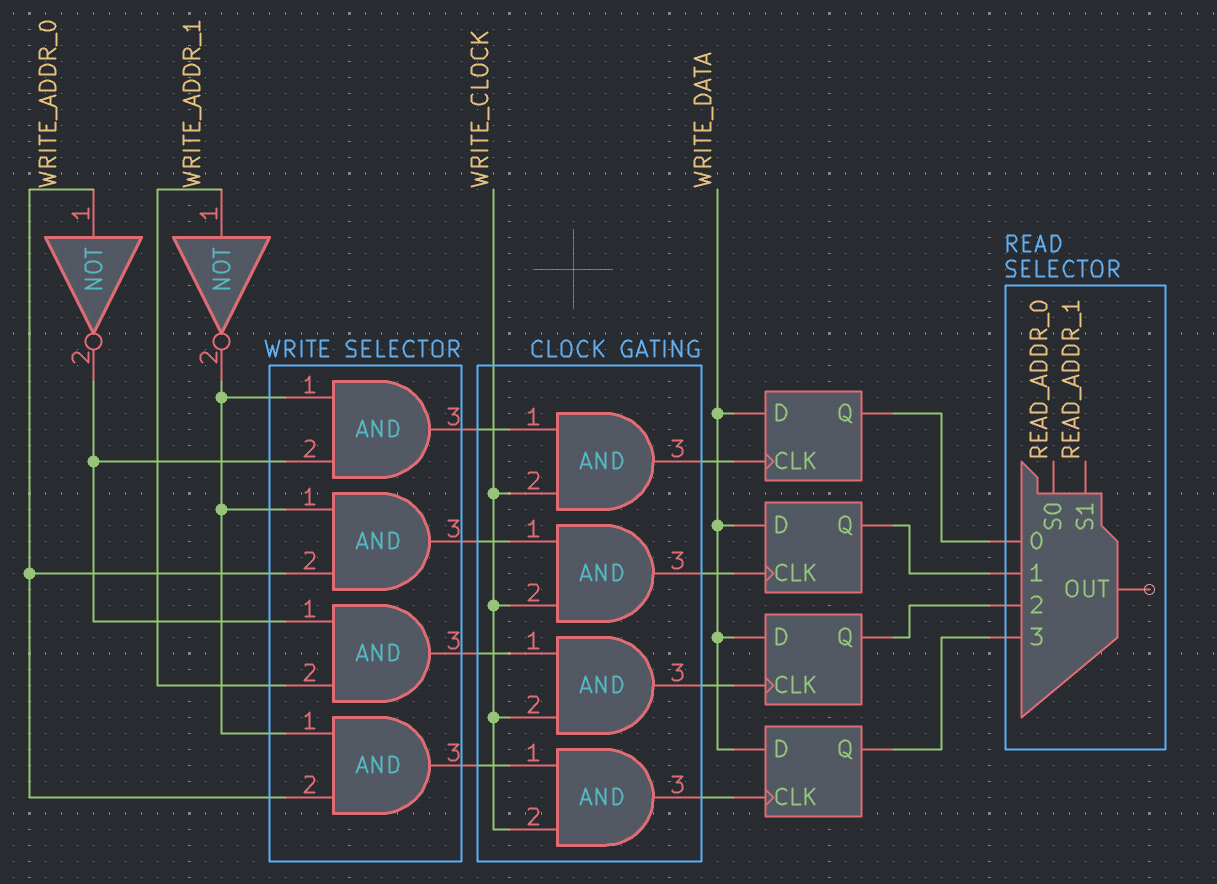
Now combine everything. Take four D latches (four one-bit cells), and wrap them with logic to write one chosen cell and read one chosen cell:
 |
|---|
| A 4-cell read/write memory. Write side: an address decoder + clock gating picks which latch captures WRITE_DATA. Read side: a 4:1 mux selects which latch's bit reaches OUT. |
Trace it:
- Write address → which cell.
WRITE_ADDR_0/_1and their inverses (the two NOT gates) feed the write selector: four AND gates, each high for exactly one of the four addresses. That's a 2-to-4 decoder - the write-side counterpart of the read mux. - Clock gating → only that cell updates. Each selector line is AND-ed with
WRITE_CLOCK, so a latch gets a clock edge only when it is both addressed and the clock fires. Every other cell is left alone and keeps its value. Gating a clock with an AND gate is exactly how you say "update this cell, now." - The store. The single selected latch captures whatever is on
WRITE_DATA; the rest hold. - Read address → which cell out. A 4:1 read mux (
READ_ADDR_0/_1as selects) passes the chosen latch'sQtoOUT.
That is addressable memory made fully concrete: decoder + clock gating to store, mux to fetch. Make each cell several bits wide and add address bits, and you have RAM - the same structure scaled up.
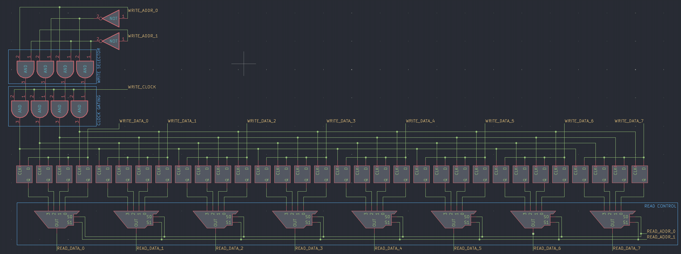
The same 4-cell bank, widened so each address stores a full 8-bit word:
 |
|---|
A 4-word × 8-bit memory. The write decoder and clock gating are shared across all eight bits of a word - the gated clock for an address clocks all eight of that word's latches at once - while each bit has its own D latch per word and its own read mux (READ_DATA_0…7). It is just the one-bit bank from above, copied eight times across the data width. |
Putting it together: a CPU
We now have every part. Assembled, they are the von Neumann machine from CS1 - for real this time:
- ALU (Arithmetic Logic Unit): the ripple-carry adder we built earlier plus logic operations, with control lines that select which operation to perform. It computes on values held in registers.
- Registers: fast on-CPU storage (the registers we built) for the values being worked on right now.
- Datapath: registers ↔ ALU ↔ memory, wired together by buses. Data flows around this loop.
- Control unit: the conductor - it produces the signals that steer everything (which register feeds the ALU, which operation runs, whether memory is read or written).
These run the fetch-decode-execute cycle from CS1, now in hardware:
- Fetch - the program counter (a register that counts) holds the address of the next instruction; the machine reads that instruction out of memory.
- Decode - the control unit reads the instruction's bits and configures the datapath.
- Execute - the ALU does the work; the result lands in a register or memory.
- The program counter advances and the cycle repeats - millions of times a second.
An "instruction" is just a number stored in memory; the control unit interprets it as a command. (How a C program becomes those numbers - the compilation toolchain - is CS1's topic, not E2's; here we assume the numbers are already in memory and watch the hardware run them.)
The microcontroller on your AirBox station is exactly this machine: a CPU with registers and an ALU, memory holding its program and data, running fetch-decode-execute to read the air-quality sensors. The diagram is the chip you'll solder.
The whole ladder: recap
Look back at what you built, all of it out of one switch:
a MOSFET switch → wired into logic gates (NOT, NAND, AND, NOR, XOR) → gates that compute (half-adder → full-adder → multi-bit adder) and, with feedback and a clock, remember (RS latch → D latch → register → memory) → all orchestrated into a CPU.
You can now read a truth table, build the basic gates from transistors, explain how a circuit adds and how a circuit remembers, and describe how memory and a CPU are assembled - closing the two questions CS1 left open (what's in a byte, how memory is built). The thread continues into CS2, where C lets you touch these addresses and bytes directly with pointers - and you've now seen the actual latches they point at.
Powering the machine: the buck converter
Everything we just built - gates, adders, memory, a CPU - only runs on clean, steady, low-voltage power; our logic lives at 3.3 V. The real world hands you messier supplies: a 12 V battery that sags and spikes, a solar panel whose voltage wanders. So we need a circuit that takes a higher, unstable input and turns it into a stable 3.3 V for the chips. The usual answer is a switching regulator, and the kind that steps voltage down is the buck converter - built, pleasingly, from parts we already know: MOSFET switches plus an inductor and a capacitor.
The circuit
 |
|---|
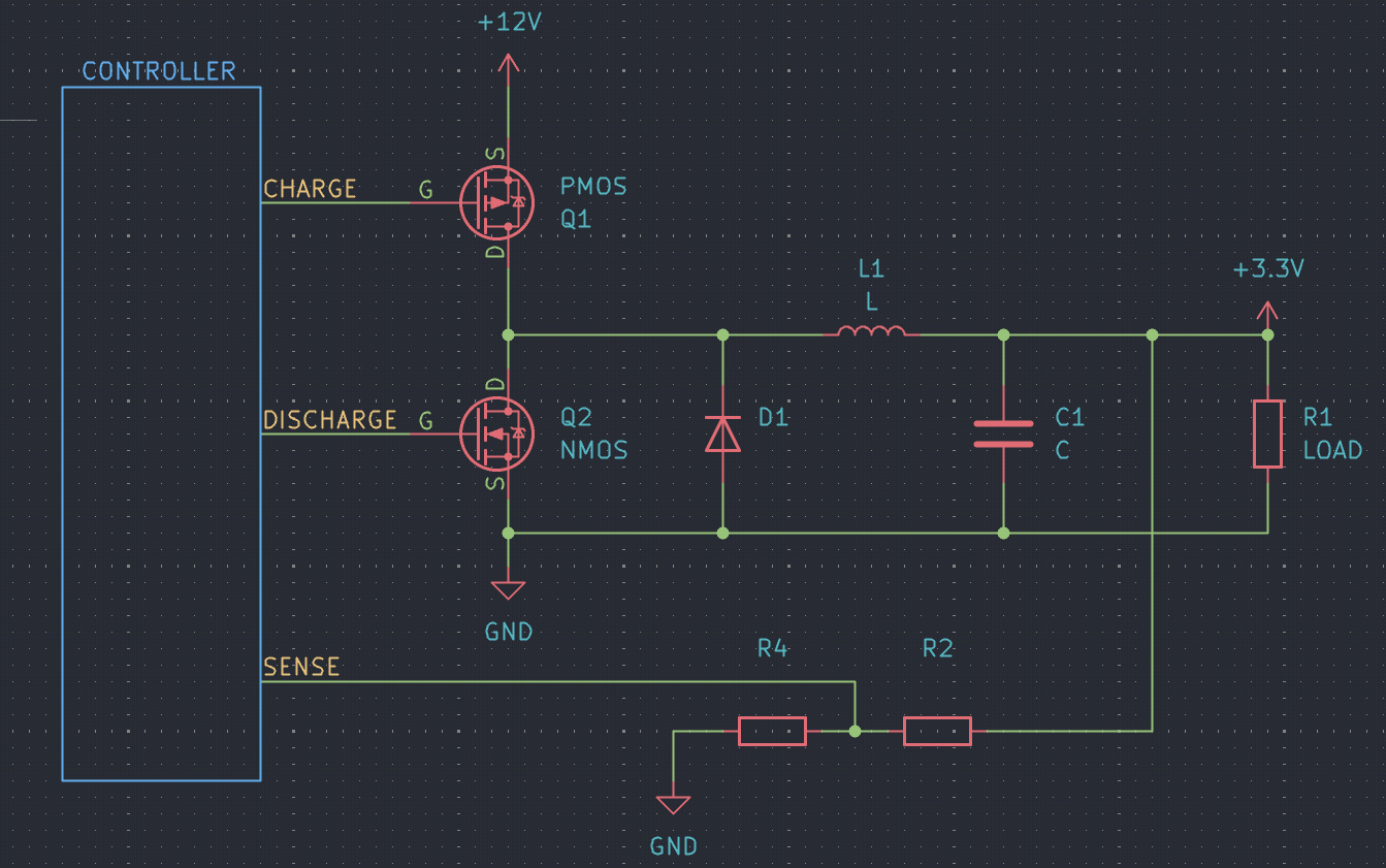
A buck converter. A controller drives two switches, watches the output through the SENSE divider, and holds the 3.3 V rail steady against a 12 V input. |
The pieces:
- Two MOSFET switches. A top switch (
Q1, PMOS, the CHARGE switch) connects the +12 V input to the inductor; a bottom switch (Q2, NMOS, the DISCHARGE switch) connects that same node to ground. (The very NMOS/PMOS pairing from earlier, doing real work.) - An L-C tank. The inductor
Land capacitorCstore energy and smooth the output - the inductor resists sudden changes in current, the capacitor holds the voltage steady for the load. - A freewheeling diode
Dthat gives the inductor's current a path to keep flowing when the top switch is off. - A controller that senses the output voltage (through the
R4/R2SENSEdivider) and decides when to pulse each switch. We won't measure how long it holds them on - just know the controller fires brief impulses to switch the MOSFETs on.
How it regulates
The controller aims at a target of 3.3 V, with guard rails at a minimum of 3.2 V and a maximum of 3.4 V.
- Charge. When the top (CHARGE) switch is pulsed on, current flows from +12 V through the inductor into the capacitor and load - energy pours into the L-C tank and the output rises.
- Coast. When that switch turns off, the inductor doesn't stop instantly: it keeps pushing its stored current through the freewheeling diode into the capacitor for a while longer. So extra energy coasts into the cap even after the switch is off, typically symmetric to the charge phase.
Two regimes follow:
- Bringing it up (light load / start-up). Each top-switch pulse lasts a fixed amount of time while the voltage is still climbing; pulse, coast, pulse, coast - the output rises in steps until it reaches the band.
- Tracking the target. Once there, the controller pulses the top switch the moment the voltage crosses the target on the way down. The charge-plus-coast then carries the output up into a small overshoot. It would be symmetric and reach near the maximum, except the load is continuously drawing energy out of the tank - so the overshoot lands a little below 3.4 V. The load then drains it back to the target, the next pulse fires, and you get a small sawtooth riding on 3.3 V.
Discharge (over-voltage protection). What if the output climbs over the maximum? That happens when the load stops drawing - or even pushes current back into the converter, like a motor coasting as a generator (regenerative braking). To stop the rail running away, the controller pulses the bottom (DISCHARGE) switch, which dumps the excess energy, pulling the capacitor back down and holding the output under 3.4 V.
Watching it work
 |
|---|
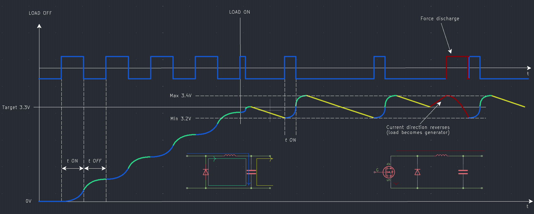
| Top: the controller's on-pulses (and, in red, a forced discharge). Bottom: the output - rising in steps while the load is OFF, then a small sawtooth around 3.3 V once the load is ON. Each phase's current is colour-coded, and the two small D-L-C drawings beneath show where the current actually flows in each phase. |
Reading the lower trace left to right:
- Load OFF (start-up): fixed-length charge pulses walk the output up in steps until it reaches the 3.2-3.4 V band.
- Load ON (normal operation): the output settles into a sawtooth - a charge pulse nudges it to an overshoot just under 3.4 V, then the load drains it down to the target, where the next pulse fires.
- Load feeds current back (the red part): when the current reverses and the load acts as a generator, the rail is driven upward; as it reaches 3.4 V the controller does a force discharge with the bottom switch to bleed off the excess and keep the rail safe.
The two little circuits beneath the graph are the same diode-inductor-capacitor section drawn twice, with arrows showing the current path in each colour-coded phase - charging, coasting, and the reverse/discharge case.
Homework
- NandGame (nandgame.com) - the main event. Starting from a single NAND, build your way up to an adder, a latch, and a CPU. It is this entire lesson, gamified and hands-on. You will have to complete the from the beginning, all the way to the end of the memory section. The Processor section is optional (Bonus points!) .
In the submission, provide a screenshot of the completion, like so:
- Short essay after finishing NandGame: what you learned and what you found hard, in your own words.
Please use.txtor.mdformats.- Practical design task - Choose an appliance in your home that you are familliar with. Something simple, with a few buttons, actuators, and some internal logic. Describe how such an appliance might be implemented using logic gates and memory components.
- Please use
.txtor.mdformats for text.- You can include diagrams, in image format. You can use Logisim for drawing and simulation.