Double-digit temperature display daughterboard
In this course we will design a live temperature display for out AirBox PCB. Our AirBox PCB contains two headers where we can connect a secondary board with any components on it.
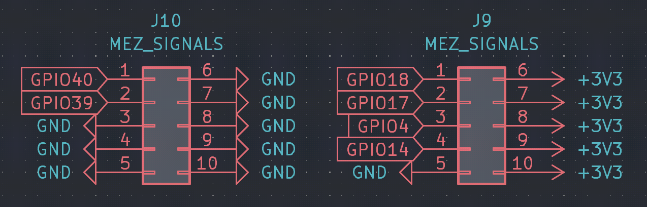
On these two headers we have exposed 6 of the ESP's GPIOs and 3.3V power pins.
 |
|---|
| J10 is near the microcontroller, J9 is towards the bottom side of the board |
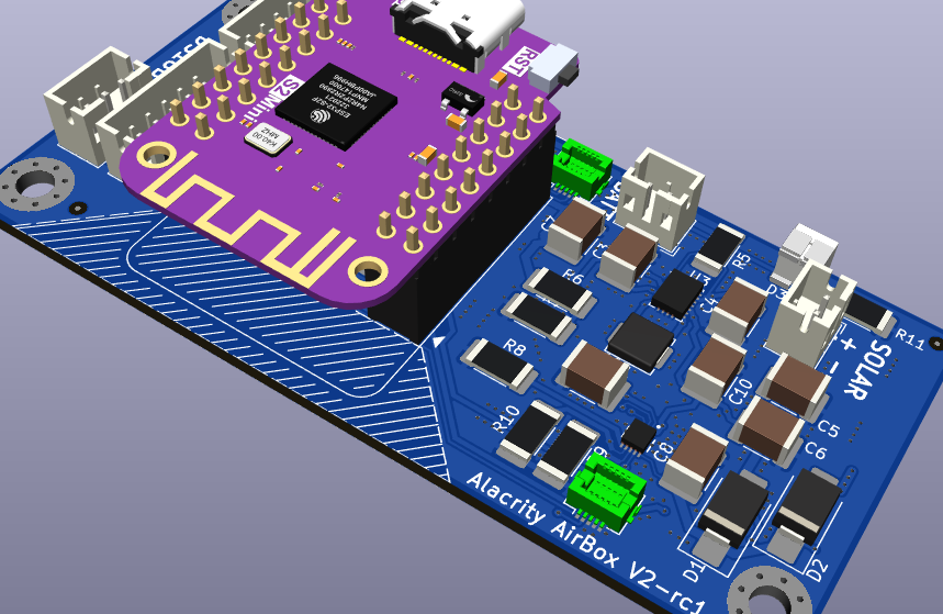
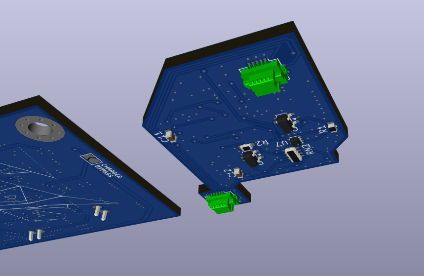
The daughterboard shape is pre-designed to fit over the power section of the AirBoxV2 and positions for the mating connectors are already in place.
 |
 |
|---|---|
| Mainboard | Daughterboard |
Design
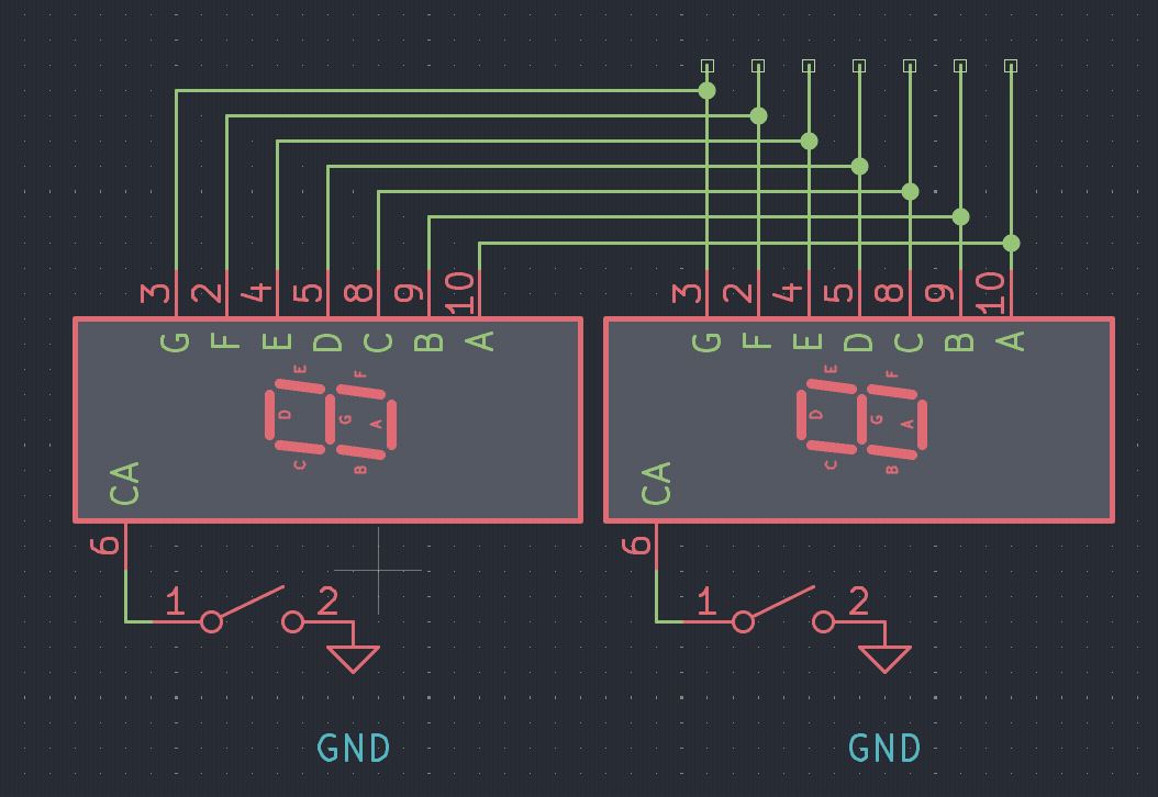
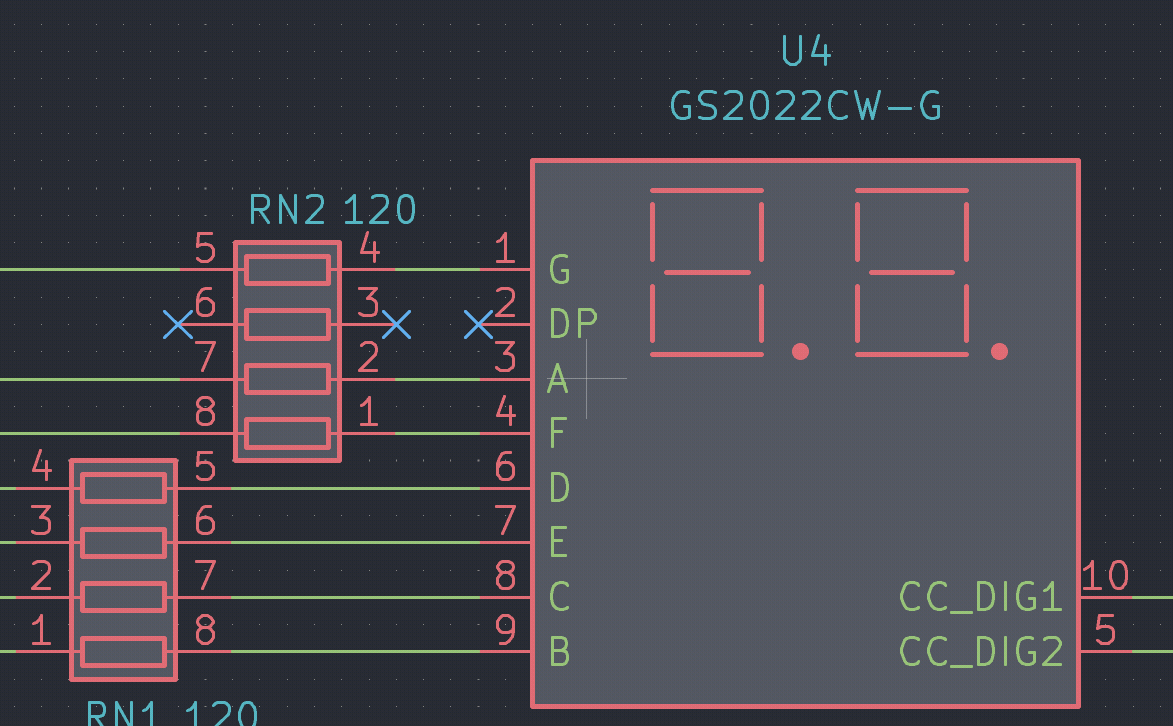
To implement a temperature display, we will use a 7-segment display. A 2-digit, 7-segment display is works by having 14 LED's (one for each line) connected into two common anode groups. Each identical segment inside the display is connected together. To display different numbers on each digit, we select (kind of like a multiplexer) which digit to activate using a MOSFET.
 |
 |
 |
|---|---|---|
A single digit is 7 LED's with all anodes tied together in the CA pin.Two digits are achieved tying the cathodes of each digit together and multiplexing. |
Equivalent representation in our AirBoxV2 daughterboard schematic. Notice the existence of current-limiting resistors arrays. |
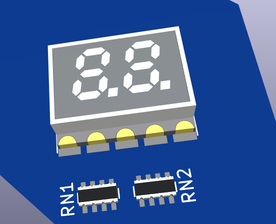
3D view of the double-digit 7-segment display with its resistor arrays. |
Total: 7+2=9 signals to drive from our code.
Now, driving each segment manually from our code is tedious. A single digit can show from 0 to 9 (10 values), a number which can be expressed in 4 bits. This fantastic chip (HEF4543B) from Nexperia allows us to transform a 4-bit number into a 7 LED states. You can see on Page 2, Fig. 2 of the datasheet its internal logic gate schematic.
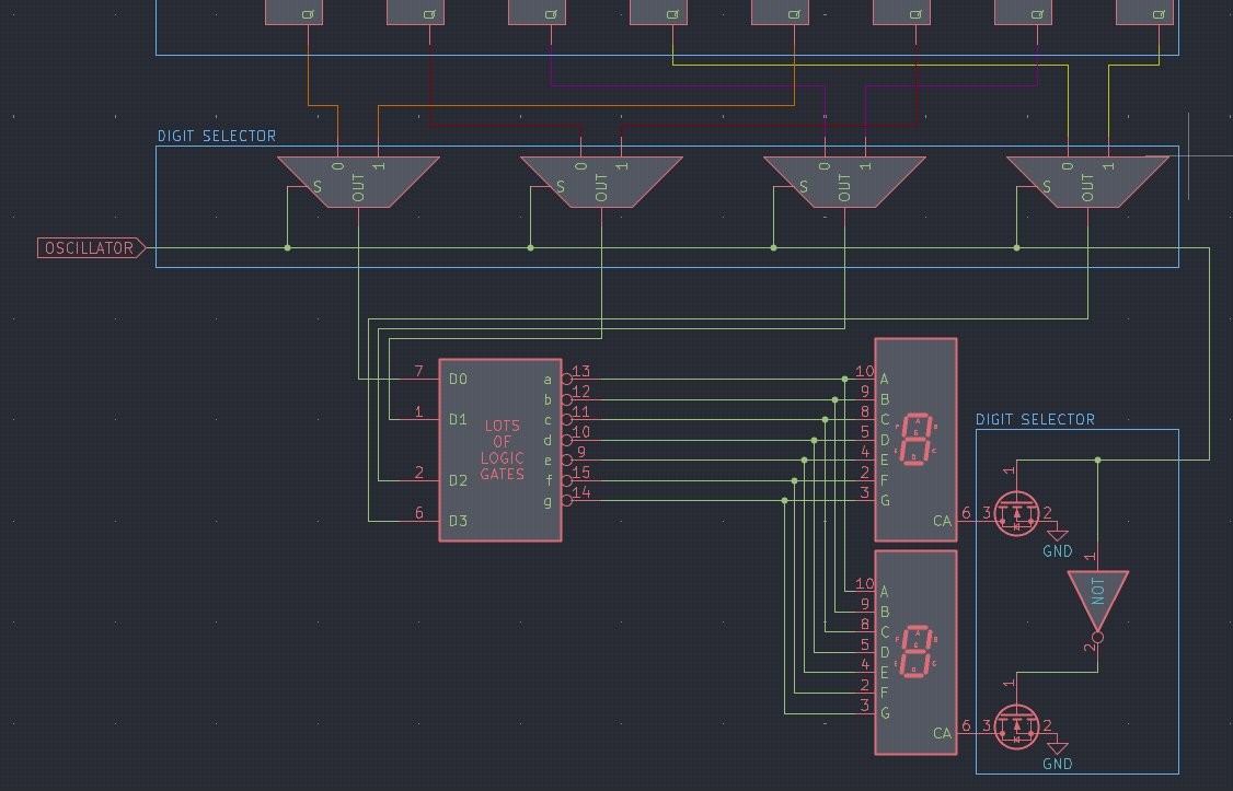
We can further combine this with 4 2:1 multiplexers, two mosfets and a fast ocsillators, and now our input becomes two 4-bit numbers, with fully automatic digit switching!
If we want to print 57, we first calculate the 8-bit number by concatenating the digits in binary:
uint8_t display = (num % 10) * 32 + num / 10;
 |
|---|
| 8-bit to double 7-segment display (input bits at the top) |
But still we don't have 8 signals available on our daughterboard. We have to find a way to compress.
Enter serial protocols!
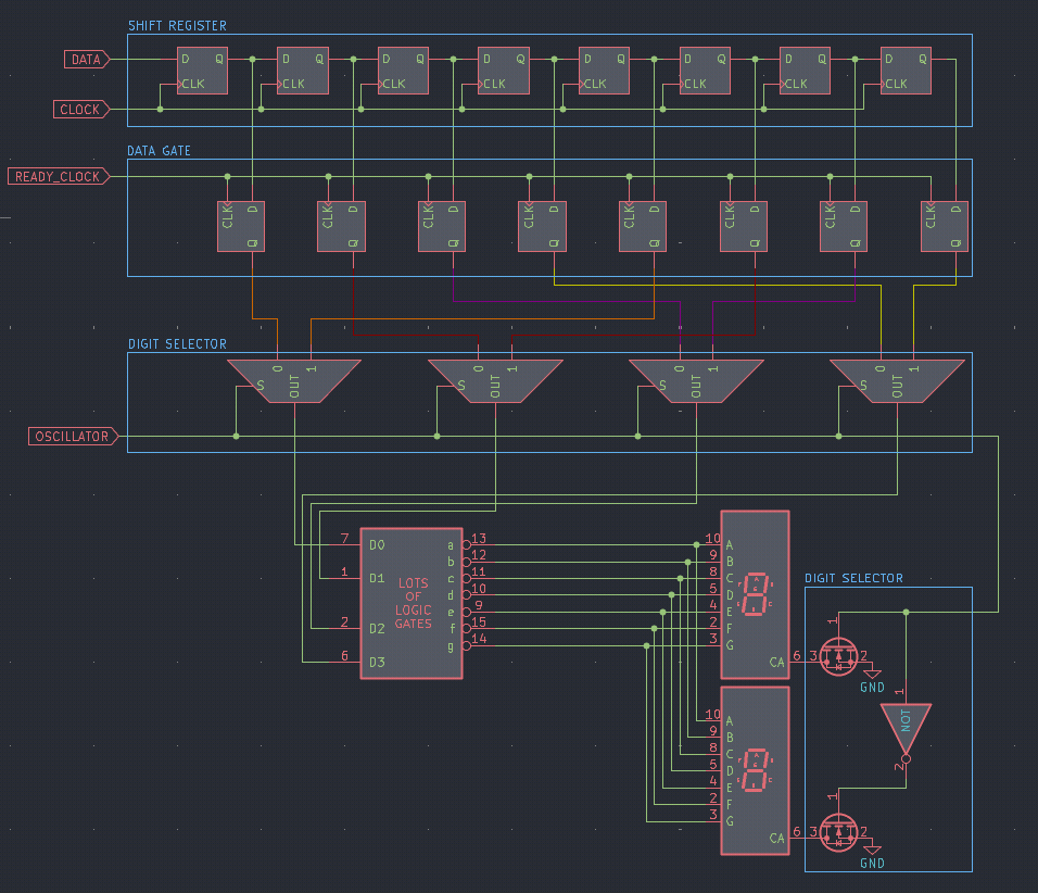
Remember the D-Flip-Flop from E2? It is the memory cell that copies the value on the D line when the clock rises, and outputs it when the clock falls.
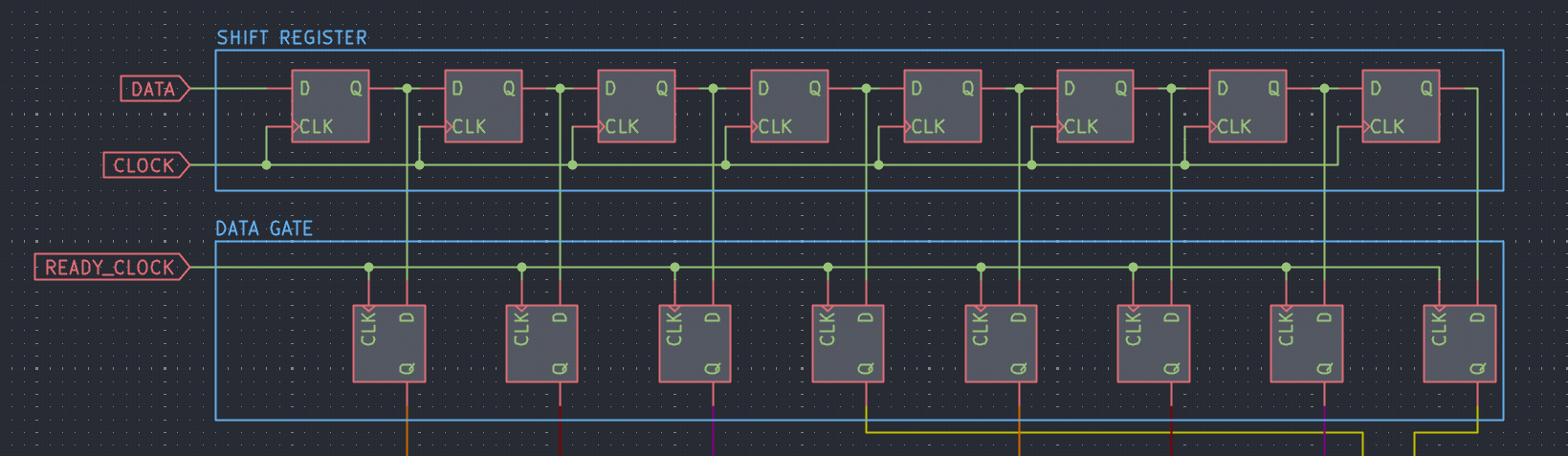
If we connect 8 of these in series, for each clock coming trough, all memory contents gets shifted to the right and the leftmost memory will copy the incoming bit over the data line.
While we are shifting new data in, the output is varying wildly, so we add another layer of Flip-Flops to present the data once we are finished with shifting.
 |
|---|
Data goes left on the CLOCK, and down on the READY_CLOCK. Only 3 signals for as many outputs as we want. |
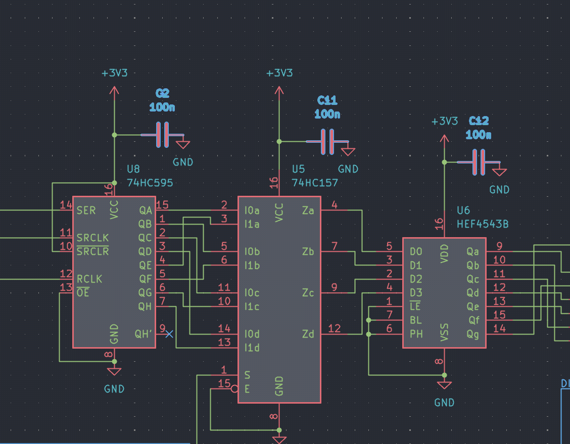
This exact construct is found inside the 74HC595 chip from Texas Instruments, which we will use a bit later on our electronic schematic.
Complete logic schematic
 |
|---|
Pseudocode for displaying a number (num) on our display:
display = (num % 10) * 32 + num / 10;
repeat 8 times:
		DATA = display % 2
    CLOCK = 1
    delay 100us
    CLOCK = 0
    delay 100us

READY_CLOCK = 1
delay 100us
READY_CLOCK = 0
Translating to electronics schematic
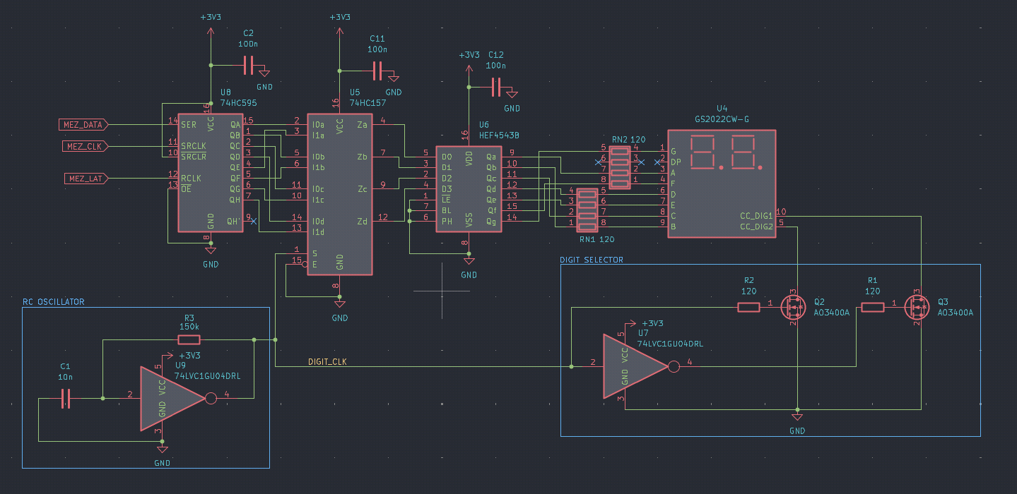
A few things change when translating from the logic to the electronic schematic. Notably:
- Most of the components need power supply (
3.3VandGND) with a decoupling capacitor. - Resistors show up on the LED lines and on MOSFET gates (which replace the previous switches)
- The four muxes are built inside a single chip (
74HC157) - The oscillator is constructed using a RC circuit (remeber E1?) and an inverter. Oscillating frequency is abut 1000Hz.
 |
|---|
In the next parts, we'll learn how to use KiCAD and turn this electronci schematic into a complete PCB with components, routing and manufacturability.
KiCAD Basics
In this section, we will be discussing essential KiCAD concepts.
We won't go into details on which buttons to press or where the options are located in the menu. Instead, there will be a cheatsheet at the bottom with shortcuts, buttons and quick references.
Workflow
KiCad's PCB design workflow centers on three tools: you define your circuit in the Schematic Editor, transfer it to the PCB Editor via "Update PCB from Schematic" to place components and route traces, and check the result in the 3D Viewer before manufacturing. When changes are needed, you edit the schematic and re-sync, keeping it as the single source of truth—then export the fabrication files to produce the board.
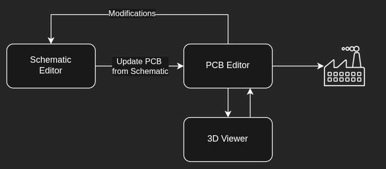
You start in the Schematic Editor, where you capture the logical design of your circuit: the components and how they're electrically connected, without worrying about physical placement.
Once the schematic is ready, you push it into the PCB Editor using the Update PCB from Schematic action. This transfers your components and their connections (the netlist) into the layout environment, where you assign footprints, arrange parts on the board, and route the copper traces that physically realize the connections you defined.
Most of the Electronics you did in school happen in the Schematic Editor stage. For the AirBoxV2 Temperature Addon, this stage is already done for you.
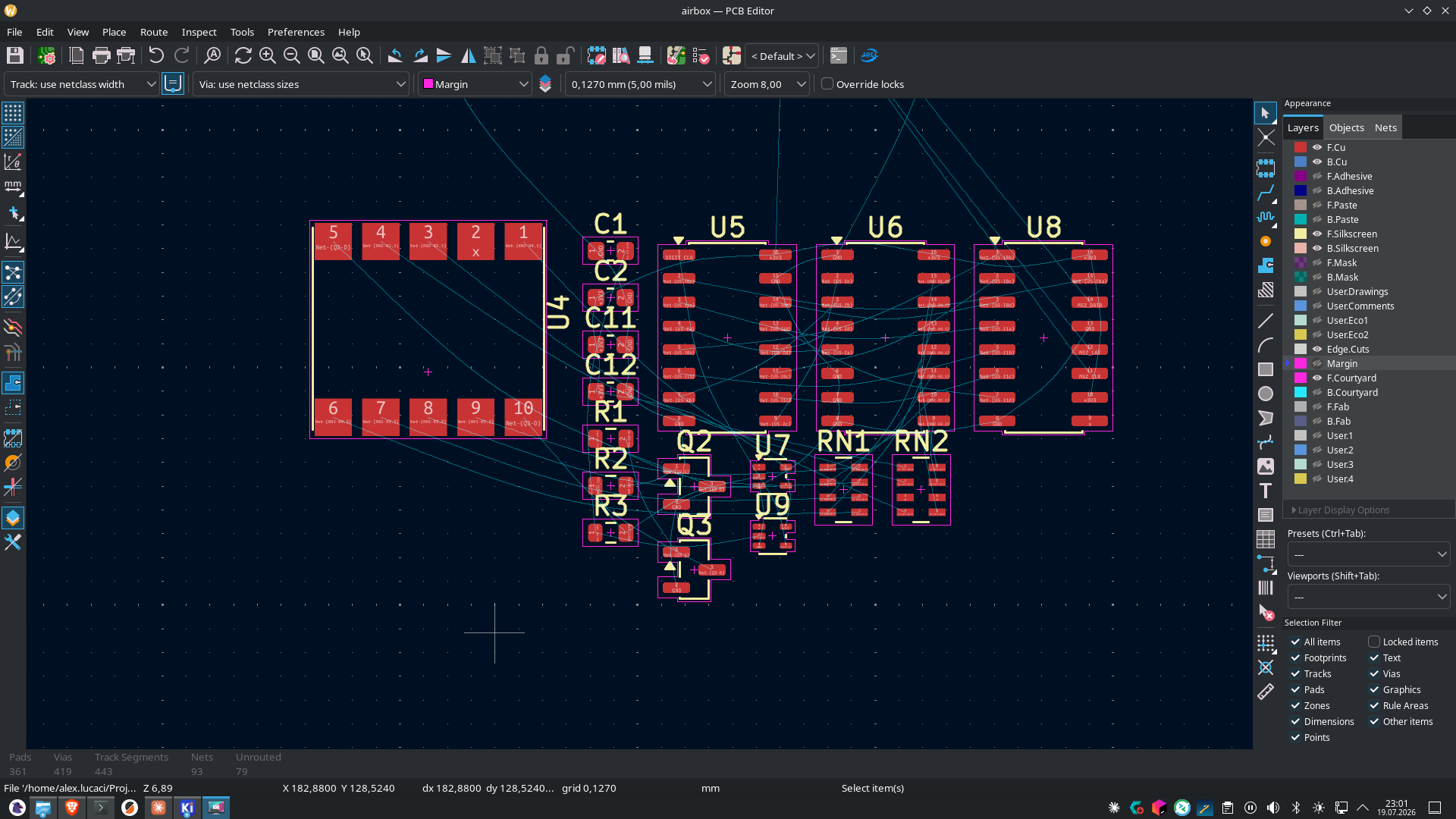
We will focus on actually routing and finishing a PCB, from a complete schematic.
 |
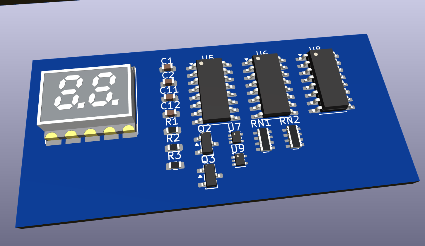 |
|---|---|
| The PCB Editor with a few un-routed components | Same components in the 3D Viewer |
Layers
A KiCad PCB is built up from a stack of distinct layers, each serving a specific purpose. Some carry the actual copper that forms your electrical connections, while others hold documentation and manufacturing information: component outlines, labels, solder mask, and clearance boundaries.
F.Cu(Front Copper, RED) is top copper layer of the board, where components are typically placed and wires/traces are routed.B.Cu(Back Copper, BLUE) is the bottom copper layer. It's used for routing traces on the underside of the board, ground planes, or mounting components on the reverse side. Connections betweenF.CuandB.Cuare made through vias (more details later).F.CourtyardandB.Courtyard(bright orange perimeters) contains the outlines of components. It is used by the design software to ensure components don't overlap.F.SilkscreenandB.Silkscreenis a drawings layer that is used to print white markings on the PCB. The white markings you see in the above pictures in the 3D view are silkscreen layers.
In KiCad you don't build a board by dropping individual elements onto separate layers.
Instead, each component is a self-contained footprint that already spans multiple layers at once:
- Copper pads live on the copper layer
- The outline and printed text is on the silkscreen
- Its keep-out zone on the courtyard
All distributed automatically when you place the part. The only layer choice you actually make is which side of the board the component sits on: top (shown in RED) or bottom (shown in BLUE). Flipping a component to the other side moves all of its associated layers together accordingly.
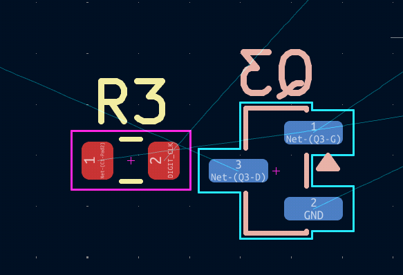 |
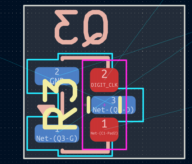 |
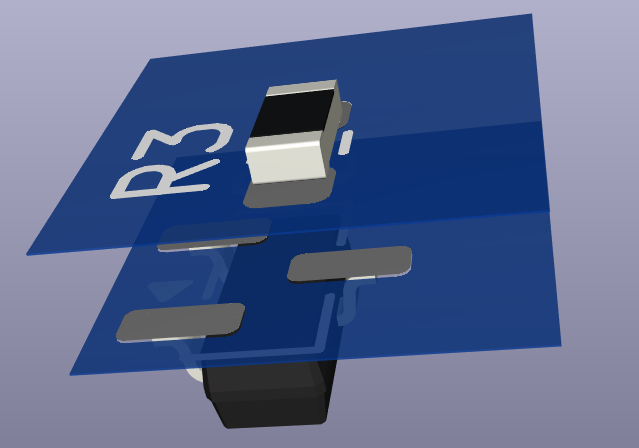 |
|---|---|---|
| A component (R3) on the Front layer (notice the RED color scheme) and another (Q3) on the Bottom layer (BLUE color scheme). Notice how the Q3 text is automatically mirrored because we are looking at the bottom layer. |
We can even place them in the same space, as long as components are in the same layer. | 3D view of the overlaid components, with the board body hidden. |
Routing
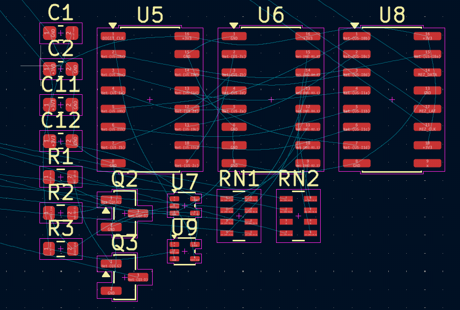
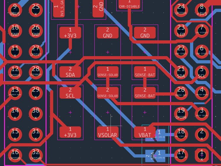
Routing is the process of drawing the copper traces that physically connect your components, realizing the electrical connections defined in the schematic. When you first update the PCB from the schematic, connections are shown only as thin straight lines called the ratsnest: these are not copper, they simply indicate which pads must be connected. Your job is to replace each ratsnest line with a real copper trace.
 |
 |
|---|---|
| Ratsnest (the thin white lines telling you what to connect) | Fully routed components (no ratsnest) |
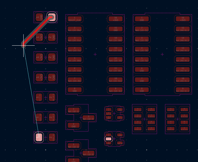
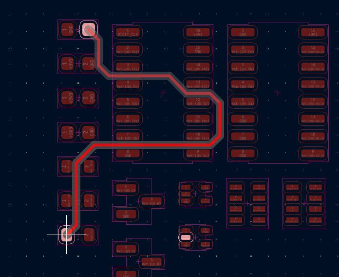
When you start routing, you will see the software help you arrive at the correct destination. It will highlight all the pads and pins where your trace must arrive at. You will also observe that KiCAD will not let you pass trough another different copper area.
 |
 |
|---|---|
| KiCAD highlighting the destination pads | Interactive router will search for a way to your destination without you having to draw all segments. |
Vias
Sometimes we need a way to route a track from a layer to another layer. We do that using what is called a via.
A via is a tiny metal-plated hole in the board body that connects two copper areas from different bodies.
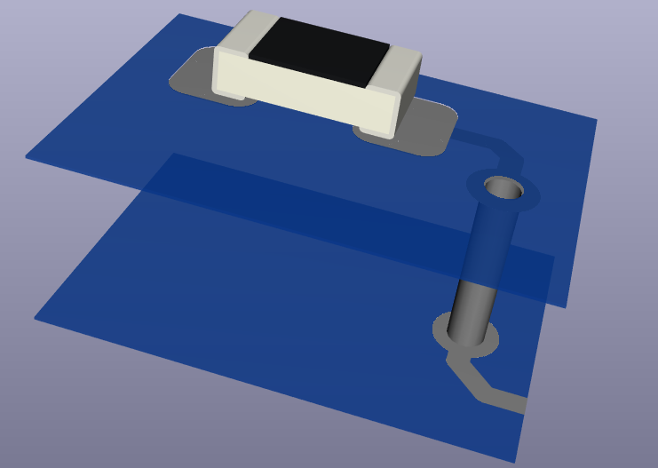 |
|---|
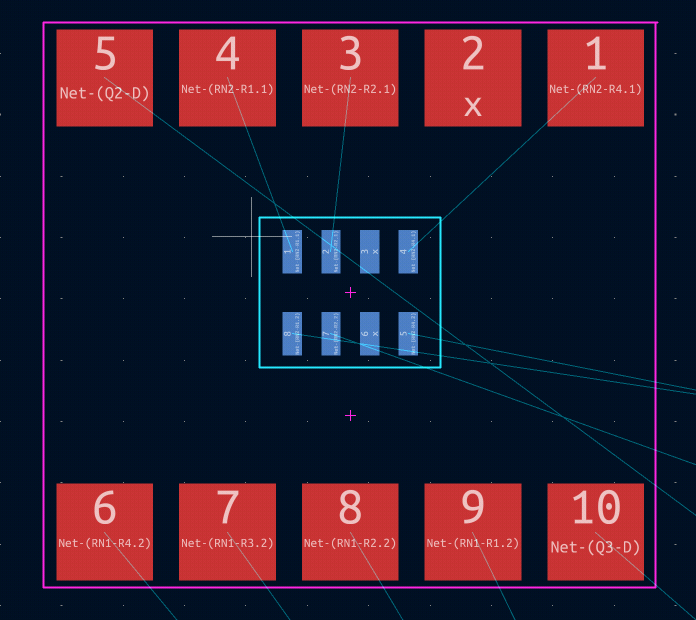
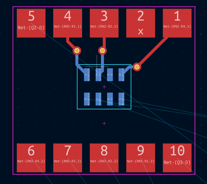
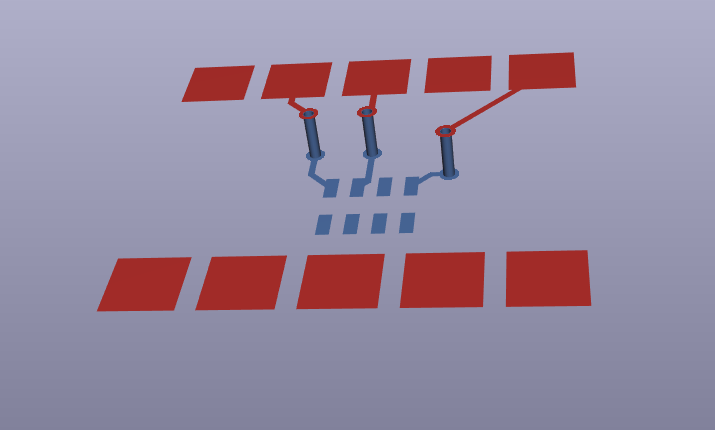
Let's see a practical example of vias:
 |
 |
 |
|---|---|---|
| We need to route pads 1, 3, 4 of the top component to the resistor array on the bottom. | Tracks and vias are used to cross the layers | 3D view of the vias with all surfaces hidden |
Copper pours
After routing all the traces with vias, we often want to fill the board's remaining space with copper. This filled region is called a copper pour (or copper zone), and it's usually connected to a common net such as GND.
Instead of routing every ground connection as an individual trace, you define a zone on a copper layer and assign it to the GND net. KiCAD then floods all the free space on that layer with copper, automatically flowing around existing traces and pads while keeping the correct clearance. Any pad on the same net is tied straight into the pour, so ground connections become short and effortless.
We often do ground copper pours because:
- Simpler grounding - Almost Every components has a GND pin and routing them all manually would take ages.
- Lower resistance to GND.
- Better heat spreading using unused board space.
A pour is a dynamic fill: it recalculates its shape to respect the traces, pads, and clearances around it. Because of this, after moving a trace or component you should refill the zones so the copper updates. If you ever see a pour that looks out of date, refill.
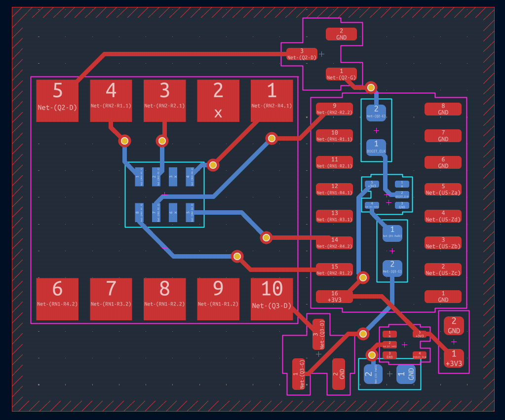 |
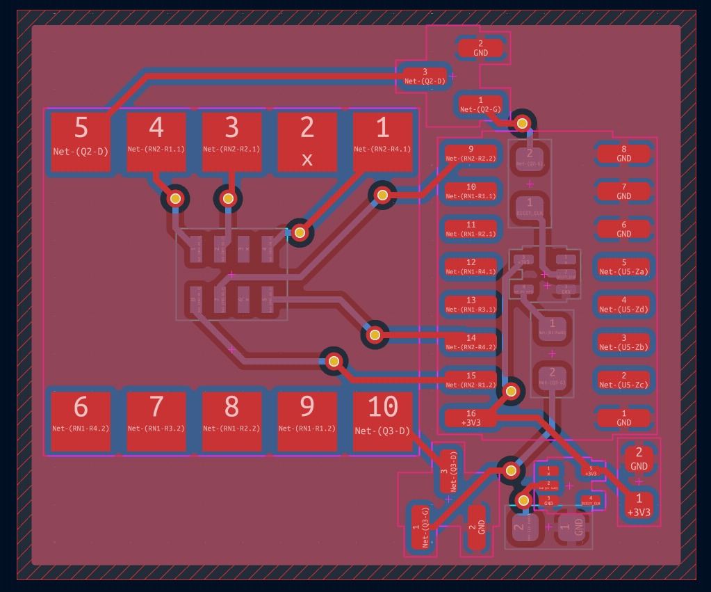 |
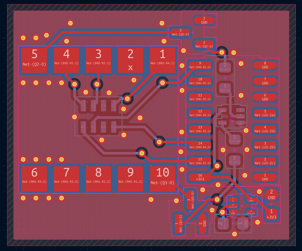 |
|---|---|---|
| A routed section inside a copper pour area (notice the edge hatching) but no copper is poured yet. | Copper poured in the respective region (after refill is activated). | We connect the two ground pours with a bunch of vias, to create a singular ground reference plane. |
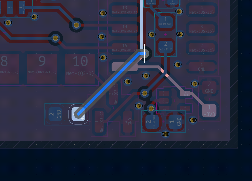
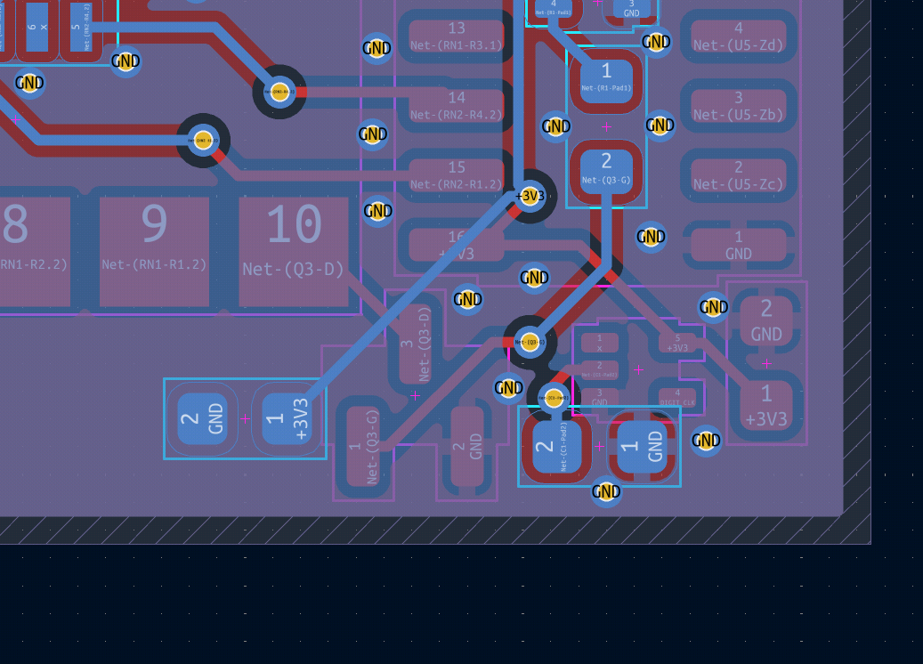
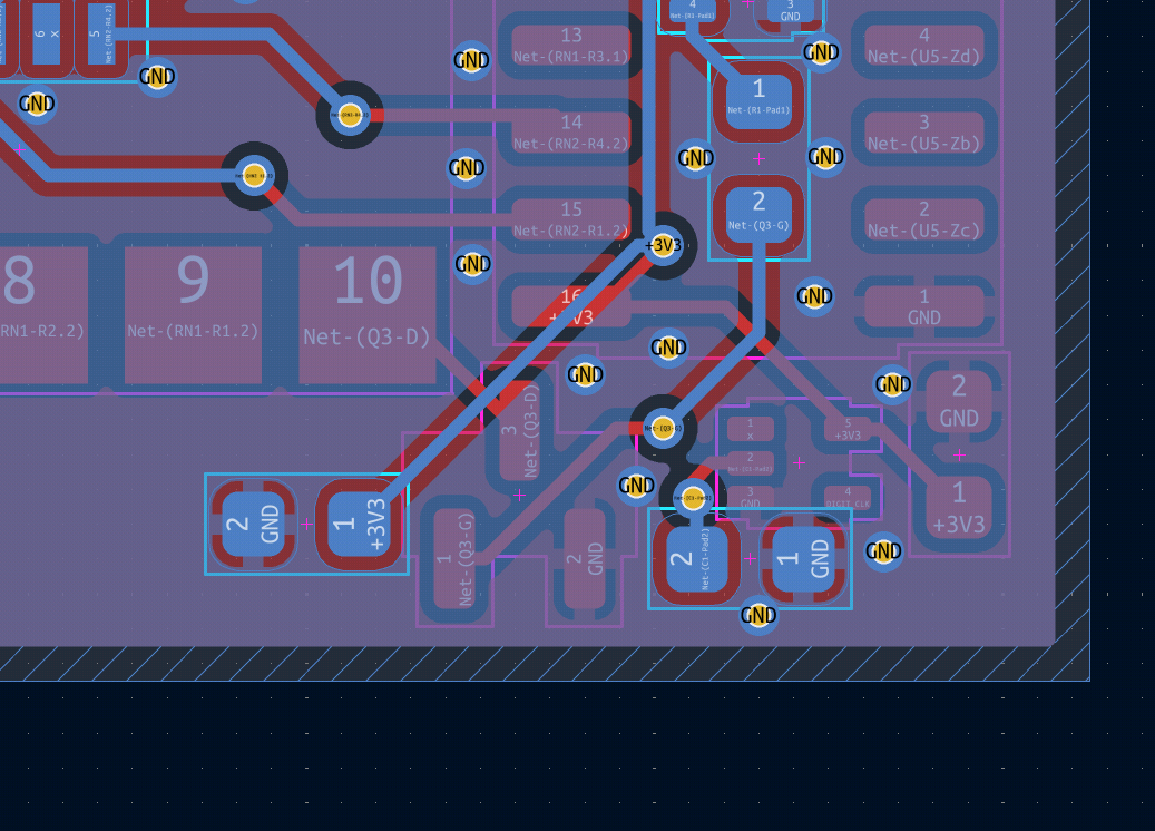
Let's see a practical example of a editing with a ground pour in place.
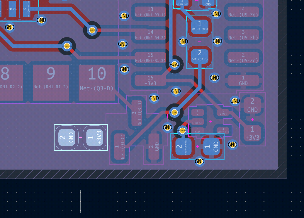 |
 |
 |
 |
|---|---|---|---|
| Place the component in the pour area. | We can draw tracks just fine over the pour. We can also put vias or do any operation even the pour is in place. | The track is finished . | Press the refill shortcut and the pours will be adjusted for new modifications. Notice how the pour is split where we drew our new track. The new component is also connected to the ground area. |
Thermal Reliefs
Thermal reliefs is a feature KiCad does automatically to help us solder component easier.
When a copper pour connects a pad, only some whiskers of that pour connect. This is to help us heat the pad using a soldering iron without having to heat the whole board.
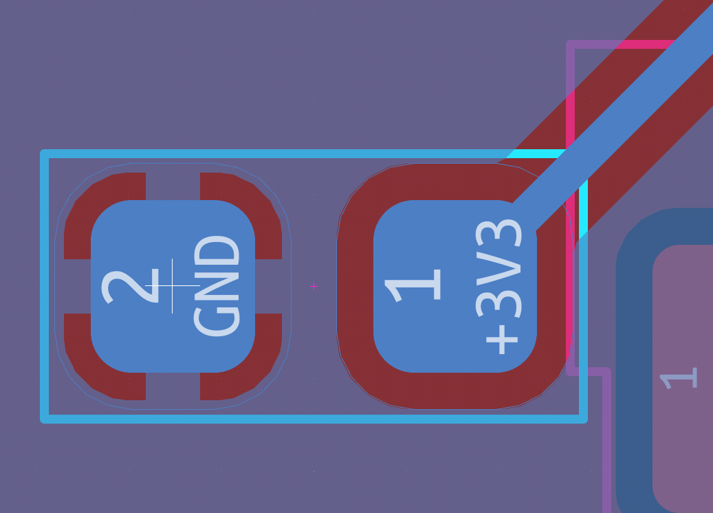 |
|---|
| Thermal Reliefs |
Our task at hand
Today's exercise is to take the AirBox Temperature Display Addon from a finished schematic all the way to a manufacturable board by doing the complete PCB layout and routing yourself. The circuit design is already captured in the Schematic Editor - your job is everything on the PCB side: placing the components, routing the signals and power, pouring and stitching the ground plane, and tidying up the silkscreen.
You are not starting from a blank board. To let you focus on layout and routing, we've prepared the following for you:
- J9 and J10 connectors are already placed in their correct positions. These are the daughterboard-to-mainboard connectors that bring in the microcontroller signals,
GND, and3.3V. - The board outline is drawn on the
Edge.Cutslayer, matching the shape that fits over the AirBoxV2 power section. - A ground pour is preconfigured over the whole daughterboard, ready to be filled once routing is done.
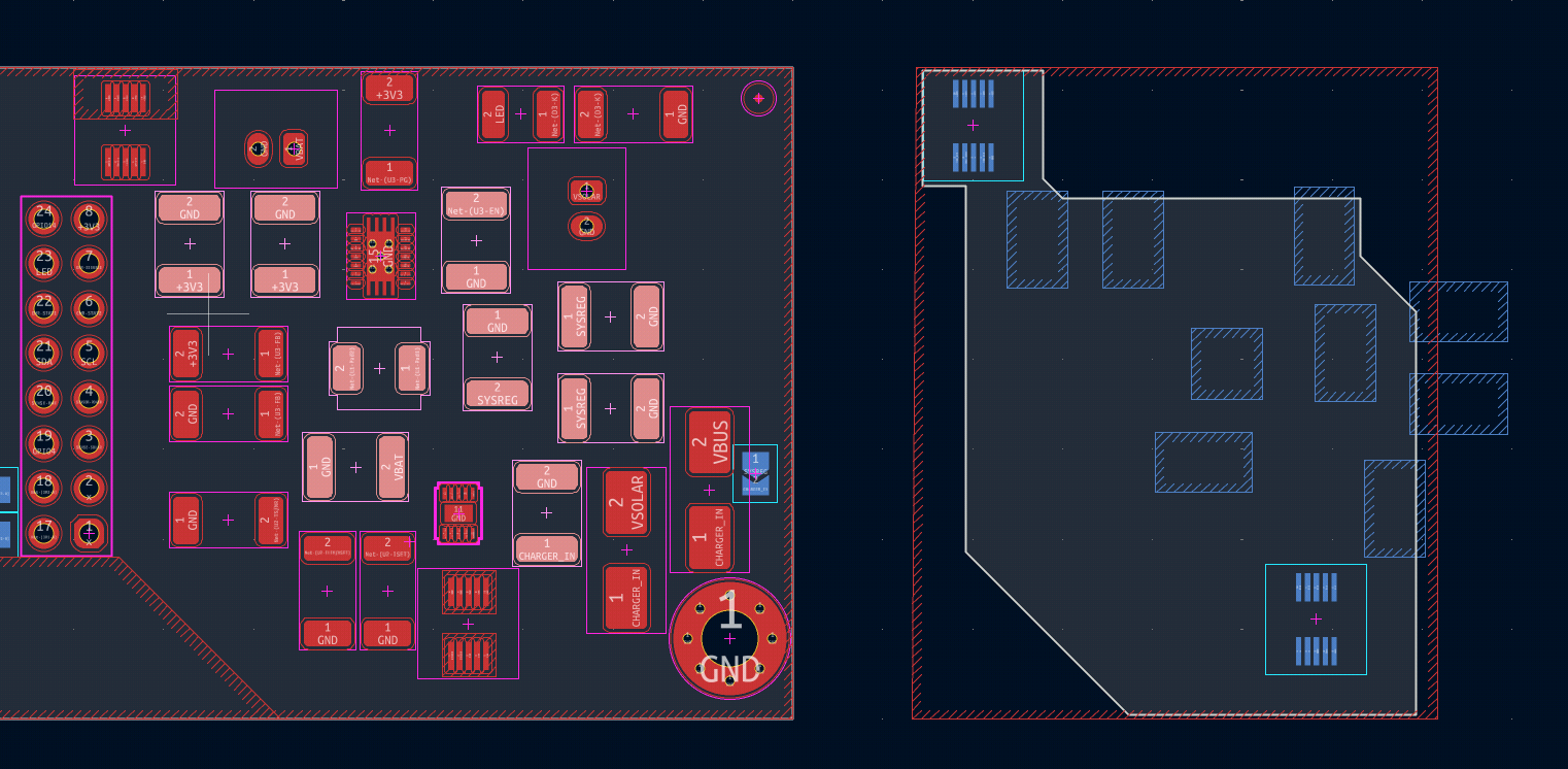
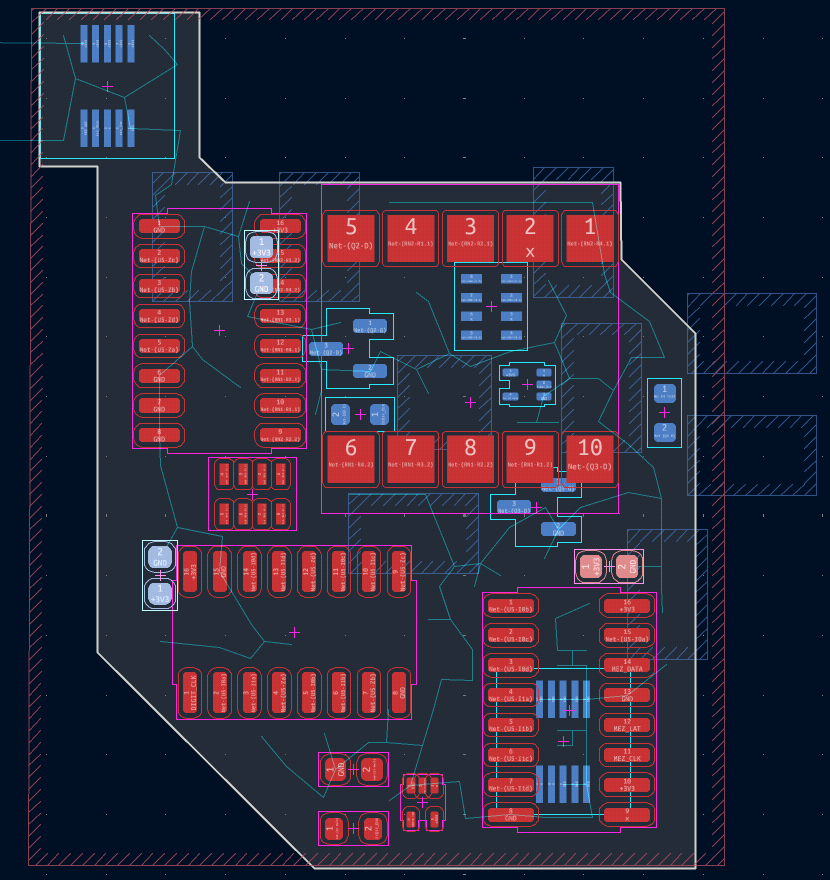
- Keep-out component zones are already defined, marking the areas where tall capacitors on the mainboard prevent you from placing components on the bottom (
B.Cu) layer.
Remember: the keep-out zones only restrict component placement on
B.Cu. You can still route tracks and drop vias freely over those areas — see the note under the image below.
 |
|---|
The little hatched rectangles are component-keep-out zones. A few capacitors on the main board are too tall and do not allow us to place components directly over them, on the B.Cu (bottom) layer. We can route tracks just fine over those areas! |
Layout
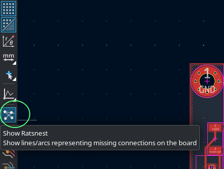
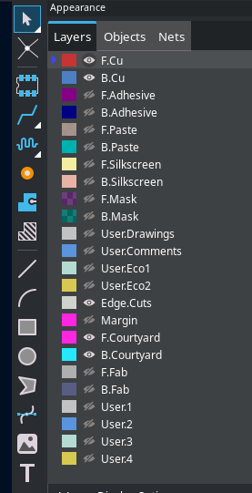
Frist, let's de-clutter our view. Hide all layers except F.Cu, B.Cu, Edge.Cuts, F.Courtyard and B.Courtyard. You will see that the PCB display will clean up a lot. We'll handle the other layers later. Then, we enable the ratsnest view.
 |
 |
|---|---|
| Enable ratsnest view | Hide all the unnecessary layers |
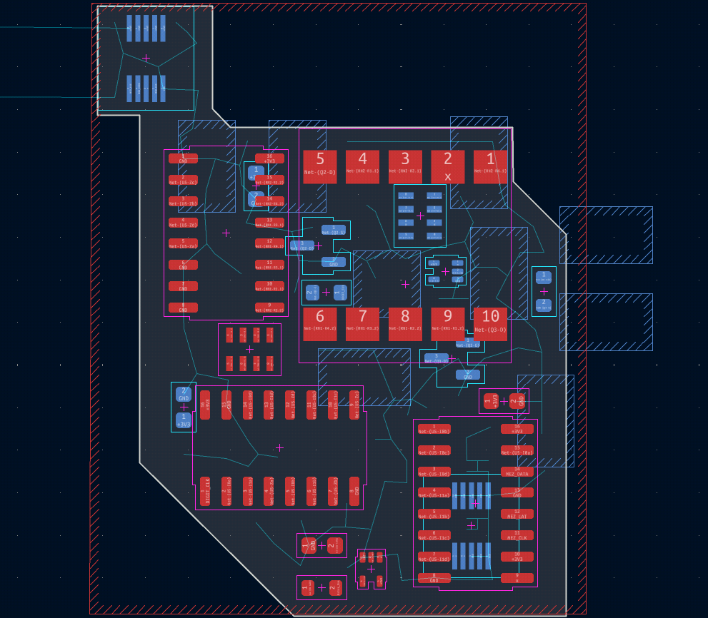
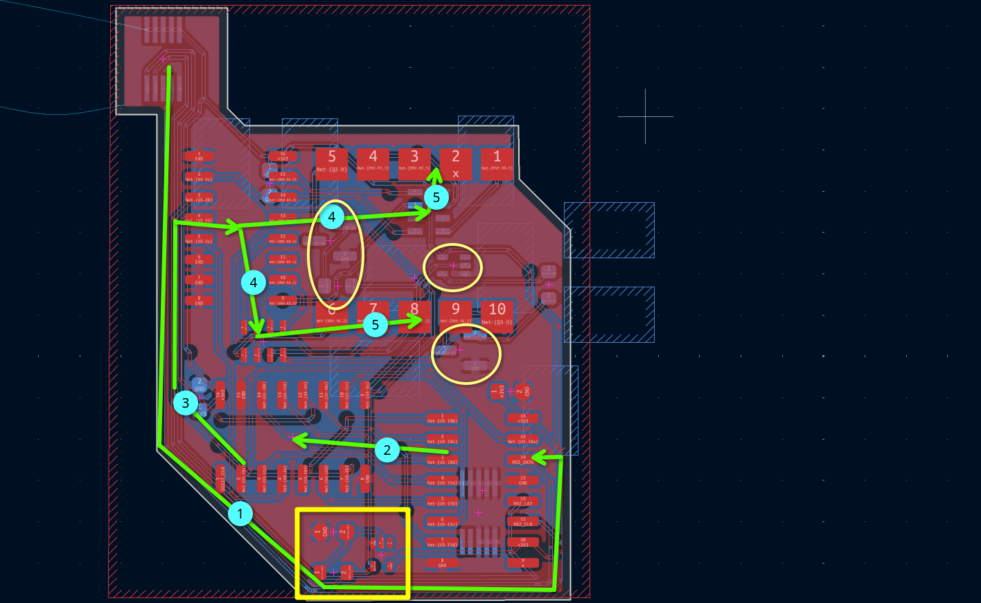
We will start by creating our component layout. We will place the components on the PCB area without routing any tracks. We will be mindful of what components groups need to stay together and which big components have connections between them. In our circuit, the data connection flow is like so:
flowchart LR
    TC[Top Connector] -->|"(1)"| SR["Shift Register (74HC595)"]
    SR -->|"(2)"| QM["Quad Mux (74HC157)"]
    QM -->|"(3)"| DD["Digit Decoder (HEF4543B)"]
    DD -->|"(4)"| R[Resistors]
    R -->|"(5)"| DISP[Display]

    RC[RC Oscillator] --> QM
    RC --> INV[Inverter]
    RC --> SW["MOSFET (AO3400)"]

    INV --> SW
    SW --> DISP
Below is an example layout. The main dataflow is highlighted in green and the connections are marked with numbers, while the oscillator and switching component locations are highlighted in yellow.
 |
 |
|---|---|
| Example component layout with no signals routed To save space, small components like inverters, MOSFET's, resistors are placed on the bottom layer, under the display. Because of the keepout restrictions, we would not be able to place the big IC's there. |
Same layout signals, routed and highlighted. Notice how components that talk are close to each other to minimize route length. |
Keep the decoupling capacitors close to their respective chips. They help with power supply stability.
 |
 |
|---|
You are highly encouraged to create your own layout.
For example, the area under the the Decoder IC can be used for other purposes, like having the oscillator together with all the switching hardware on theB.Culayer, freeing up some area in the lower section. Or you can place the shift register near the data connector, go left with the muxes and then down with decoder and display.
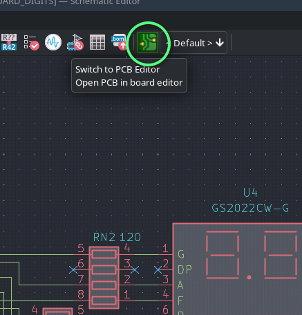
How do we identify a component as its place in the schematic? Or how do we locate a specific component on the schematic, on the PCB editor? Worry not, KiCAD has a simple fix:
Each editor has a button to switch to the other editor. Select a component (or a pad) and press the switch button. You will be transported to the other editor with that specific element focused.
 |
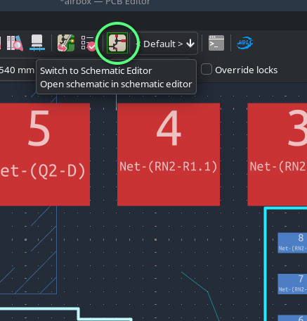 |
|---|---|
| Select a schematic element and press the button to see its location on the PCB | Select a PCB elements to see its schematic counterpart |
Routing
Now that we have ensured components are placed at conveninent positions, let's start routing the signals. First, prepare for routing by selecting the correct track width and via size:
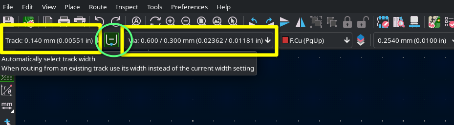 |
||
|---|---|---|
Select track width as 0.14mm or 0.2mm for signals, thicker for power |
Unselect the "Automatically select track width" option | Select via size as 0.6mm (copper ring) / 0.3mm (hole) |
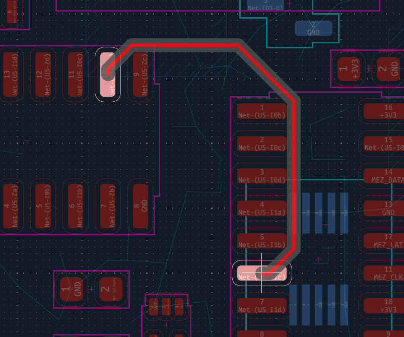 |
|---|
| Route your first signal. Continue with the others. |
Ignore
GNDand3.3Vnets for now. Those will be provided by the power traces and ground fill we'll connect later.
Once you are finished with signals, it's time to connect 3.3V power to the components. Because on this PCB we are dealing with very small currents, we do not need to make very think traces for power.
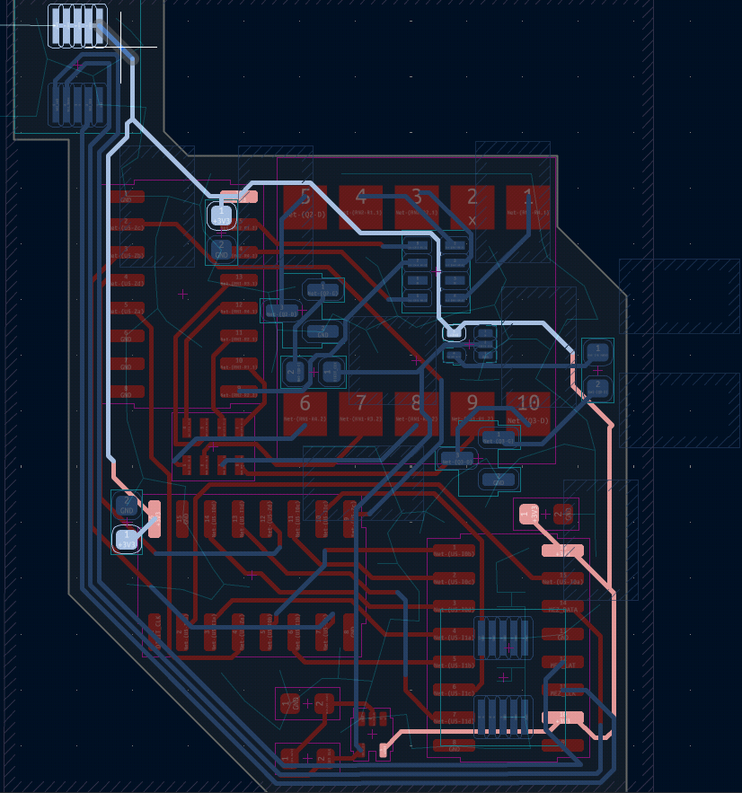 |
|---|
| Example power strip routing. |
GND pour
One single net unrouted remains: GND.
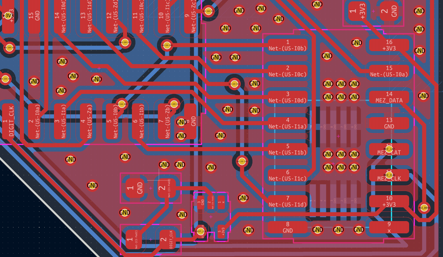
Simply press B to pour GND on all empty voids. Copper floods the board, but does not ensure copper continuity. We will continue by adding vias to the copper pour to ensure continuity across the two layers.
 |
|---|
Vias are added all over the GND plane to connect front to back regoins. This technique is called "Via stitching". |
Silkscreen
Enable the F.Silkscreen and B.Silkscreen layers. Look at where the reference designators are drawn and move them so that the labelling is clear.
It is OK to remove labels if they do not fit the layout. You can also draw arrows, lines, and helper designations using the drawing tools on the right side of the screen.
KiCad Cheatsheet
| Action | Shortcut |
|---|---|
| Select | L CLICK or L CLICK + Drag to create a selection box. Dragging left-to-right selects only items fully enclosed by the box, while dragging right-to-left selects anything the box touches or crosses. |
| Unselect | ESC |
| Move selection | M, then move the mouse and click when finished |
| Flip selection top/bottom | Select, then F |
| (Re)Generate copper pours | B |
| Ungenerate copper pours | CTRL + B |
| Expand selection to the whole net | U |
| Switch active layer (top/bottom) | V |
| Route tracks | Mouse over the starting pad/position, then X (see routing steps below) |
Once routing is active (after X):
| While routing | Action |
|---|---|
| Move the mouse | Route toward where you want to go |
| V | Cross layers using a via, then L CLICK to place the via and continue on the other layer |
| L CLICK over destination | Finish the track |
| L CLICK over void | Place a waypoint and continue |
| L CLICK + L CLICK over void | Finish the track |